SPAS093C December 2009 – September 2015 TPS2505
PRODUCTION DATA.
- 1 Features
- 2 Applications
- 3 Description
- 4 Revision History
- 5 Pin Configuration and Functions
-
6 Specifications
- 6.1 Absolute Maximum Ratings
- 6.2 ESD Ratings
- 6.3 Recommended Operating Conditions
- 6.4 Thermal Information
- 6.5 Electrical Characteristics (Shared Boost, LDO and USB)
- 6.6 Electrical Characteristics (Boost Only)
- 6.7 Electrical Characteristics (USB1/2 Only)
- 6.8 Electrical Characteristics (LDO and Reset Only)
- 6.9 Recommended External Components
- 6.10 Dissipation Ratings
- 6.11 Typical Characteristics
- 7 Parameter Measurement Information
-
8 Detailed Description
- 8.1 Overview
- 8.2 Functional Block Diagram
- 8.3
Feature Description
- 8.3.1 PGND
- 8.3.2 IN
- 8.3.3 EN
- 8.3.4 GND
- 8.3.5 ILIM1/2
- 8.3.6 RESET
- 8.3.7 LDOOUT
- 8.3.8 LDOIN
- 8.3.9 ENLDO
- 8.3.10 FAULT1/2
- 8.3.11 ENUSB1/2
- 8.3.12 USB1/2
- 8.3.13 AUX
- 8.3.14 SW
- 8.3.15 Thermal Pad
- 8.3.16 Boost Converter
- 8.3.17 USB Switches
- 8.3.18 3.3-V LDO
- 8.3.19 Reset Comparator
- 8.3.20 Thermal Shutdown
- 8.3.21 Component Recommendations
- 8.4 Device Functional Modes
-
9 Application and Implementation
- 9.1 Application Information
- 9.2
Typical Application
- 9.2.1 Design Requirements
- 9.2.2 Detailed Design Procedure
- 9.2.3 Application Curves
- 10Power Supply Recommendations
- 11Layout
- 12Device and Documentation Support
- 13Mechanical, Packaging, and Orderable Information
Package Options
Mechanical Data (Package|Pins)
- RGW|20
Thermal pad, mechanical data (Package|Pins)
- RGW|20
Orderable Information
9 Application and Implementation
NOTE
Information in the following applications sections is not part of the TI component specification, and TI does not warrant its accuracy or completeness. TI’s customers are responsible for determining suitability of components for their purposes. Customers should validate and test their design implementation to confirm system functionality.
9.1 Application Information
The TPS2505 is a USB switch device enabling a 5-V supply from a single Li-Ion battery, regulated supply, or 2- to 3-cell NiCd , NiMH, or alkaline. This device is targeted toward keyboard, printer, camera, picture frame applications, and other handheld or remote applications.
9.2 Typical Application
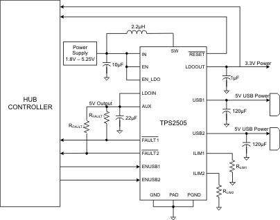
9.2.1 Design Requirements
For this design example, use the parameters listed in Table 2 as the input parameters.
Table 2. Design Parameters
| PARAMETER | EXAMPLE VALUE |
|---|---|
| Input voltage range (VIN) | 2.7 V to 4.2 V |
| AUX voltage (VAUX) | 5.1 V (internally fixed) |
| Input ripple voltage (ΔVIN) | 15 mV |
| AUX ripple voltage (ΔVAUX) | 50 mV |
| AUX current (IAUX) | 0.3 A |
| LDO current (ILDO) (powered from AUX) | 0.1 A |
| USB1 current (IUSB1 ) | 0.5 A |
| USB2 current (IUSB2 ) | 0.1 A |
| Total current (ITOTAL = IAUX + ILDO + IUSB1 + IUSB2) | 1 A |
| Efficiency target, nominal | 90% |
| Switching frequency (fSW) | 1 MHz |
9.2.2 Detailed Design Procedure
9.2.2.1 Step-by-Step Design Procedure
The following design procedure provides an example for selecting component values for the TPS2505.
The following design parameters are needed as inputs to the design process.
- Input voltage range
- Output voltage on AUX
- Input ripple voltage
- Output ripple voltage on AUX
- Output current rating of AUX rail
- Output current rating of USB rail
- Nominal efficiency target
- Operating frequency
A power inductor, input and output filter capacitors, and current-limit threshold resistor are the only external components required to complete the TPS2505 boost-converter design. The input ripple voltage, AUX ripple voltage, and total output current affect the selection of these components.
9.2.2.2 Switching Frequency
The switching frequency of the TPS2505 is internally fixed at 1 MHz for the specified VIN range.
9.2.2.3 AUX Voltage
The AUX voltage of the TPS2505 is internally fixed at 5.1 V.
9.2.2.4 Determine Maximum Total Current (IAUX + ILDO + IUSB1 + IUSB2 )
Using Figure 1, the maximum total current at VIN = 2.7 V is 1 A using the conservative line. The design requirements are met for this application.
9.2.2.5 Power Inductor
The inductor ripple current, Δi, should be at least 20% of the average inductor current to avoid erratic operation of the peak-current-mode PWM controller. Assume an inductor ripple current, Δi, which is 30% of the average inductor current and a power-converter efficiency, η, of 90%. Using the minimum input voltage, the average inductor current at VIN = 2.7 V is:

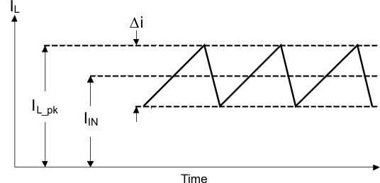 Figure 11. Waveform of Current in Boost Inductor
The corresponding inductor ripple current is:

Verify that the peak inductor current is less than the 3-A peak switch current:

The following equation estimates the duty cycle of the low-side SWN MOSFET:

where
- RSWN is the low-side control MOSFET ON-resistance
- RSWP is the high-side synchronous MOSFET ON-resistance
- RL is an estimate of the inductor DC resistance
The following equation calculates the recommended inductance for this design.

The RMS inductor current is:

Select a Coilcraft LPS4018-222ML inductor. This 2.2-µH inductor has a saturation current rating of 2.7 A and an RMS current rating of 2.3 A. See Component Recommendations for specific additional information.
9.2.2.6 Output AUX Capacitor Selection
The AUX output capacitor, CAUX, discharges during the PWM MOSFET on-time, resulting in an output ripple voltage of ΔVAUX. ΔVAUX is largest at maximum load current.


Ceramic capacitors exhibit a DC bias effect, whereby the capacitance falls with increasing bias voltage. The effect is worse for capacitors in smaller case sizes and lower voltage ratings. X5R and X7R capacitors exhibit less DC bias effect than Y5V and Z5U capacitors.
Select a TDK C3225X5R1A226M 22-µF, 10-V X5R ceramic capacitor to allow for a 50% drop in capacitance due to the DC bias effect. See Component Recommendations for specific additional information.
9.2.2.7 Output USB1/2 Capacitor Selection
The USB1/2 output capacitors provide energy during a load step on the USB outputs. The TPS2505 does not require a USB output capacitor, but many USB applications require that downstream-facing ports be bypassed with a minimum of 120-μF, low-ESR capacitance.
Select a Panasonic EEVFK1A151P 150-μF, 10-V capacitor.
9.2.2.8 Input Capacitor Selection
The ripple current through the input filter capacitor is equal to the ripple current through the inductor. If the ESL and ESR of the input filter capacitor are ignored, then the required input filter capacitance is:

Select a TDK C2012X5R1A106K 10-µF, 10-V, X5R, size 805 ceramic capacitor. The capacitance drops 20% at 3.3-V bias, resulting in an effective capacitance of 8 µF.
An additional 0.1-µF ceramic capacitor should be placed locally from IN to GND to prevent noise from coupling into the device if the input capacitor cannot be located physically near to the device.
In applications where long, inductive cables connect the input power supply to the device, additional bulk input capacitance may be necessary to minimize voltage overshoot. See Component Recommendations for specific additional information.
9.2.2.8.1 Current-Limit Threshold Resistor RILIM
The current-limit threshold IOS of the power switches are externally adjustable by selecting the RILIM1/2 resistors. To eliminate the possibility of false tripping, RILIM1/2 should be selected so that the minimum tolerance of the current-limit threshold is greater than the maximum specified USB load, IUSB.
It is also important to account for IOS shifts due to variation in VIN and IAUX. This shift due to the additional loading in AUX can add up to ±75 mA of variation to the IOS as calculated according to Programming the Current-Limit Threshold Resistor RILIM. Select RILIM1 so that the minimum current-limit threshold equals 600 mA to ensure a minimum IUSB1 current-limit threshold of 525 mA. In the same way, select RILIM2 so that the minimum current-limit threshold equals 200 mA to ensure a minimum IUSB2 current-limit threshold of 125 mA.


Choose the next smaller 1% resistor, which are 34.8 kΩ for RLIM1 and 95.3 kΩ for RLIM2.
9.2.3 Application Curves
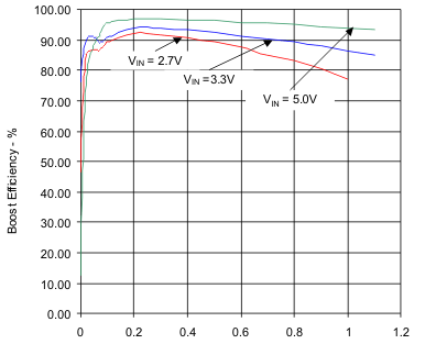 Figure 12. Boost Efficiency vs Output Current
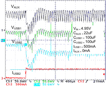
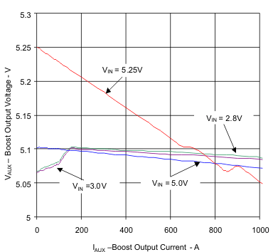 Figure 13. Boost Output Voltage vs Load Current
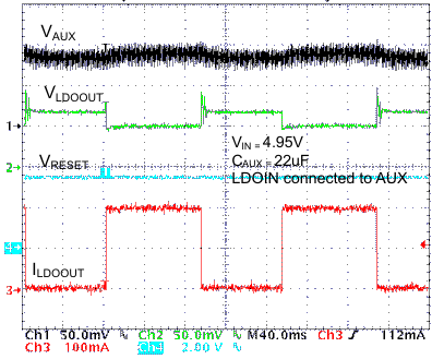 Figure 15. LDO Load Transient Response 0 mA - 200 mA