SPAS093C December 2009 – September 2015 TPS2505
PRODUCTION DATA.
- 1 Features
- 2 Applications
- 3 Description
- 4 Revision History
- 5 Pin Configuration and Functions
-
6 Specifications
- 6.1 Absolute Maximum Ratings
- 6.2 ESD Ratings
- 6.3 Recommended Operating Conditions
- 6.4 Thermal Information
- 6.5 Electrical Characteristics (Shared Boost, LDO and USB)
- 6.6 Electrical Characteristics (Boost Only)
- 6.7 Electrical Characteristics (USB1/2 Only)
- 6.8 Electrical Characteristics (LDO and Reset Only)
- 6.9 Recommended External Components
- 6.10 Dissipation Ratings
- 6.11 Typical Characteristics
- 7 Parameter Measurement Information
-
8 Detailed Description
- 8.1 Overview
- 8.2 Functional Block Diagram
- 8.3
Feature Description
- 8.3.1 PGND
- 8.3.2 IN
- 8.3.3 EN
- 8.3.4 GND
- 8.3.5 ILIM1/2
- 8.3.6 RESET
- 8.3.7 LDOOUT
- 8.3.8 LDOIN
- 8.3.9 ENLDO
- 8.3.10 FAULT1/2
- 8.3.11 ENUSB1/2
- 8.3.12 USB1/2
- 8.3.13 AUX
- 8.3.14 SW
- 8.3.15 Thermal Pad
- 8.3.16 Boost Converter
- 8.3.17 USB Switches
- 8.3.18 3.3-V LDO
- 8.3.19 Reset Comparator
- 8.3.20 Thermal Shutdown
- 8.3.21 Component Recommendations
- 8.4 Device Functional Modes
-
9 Application and Implementation
- 9.1 Application Information
- 9.2
Typical Application
- 9.2.1 Design Requirements
- 9.2.2 Detailed Design Procedure
- 9.2.3 Application Curves
- 10Power Supply Recommendations
- 11Layout
- 12Device and Documentation Support
- 13Mechanical, Packaging, and Orderable Information
Package Options
Mechanical Data (Package|Pins)
- RGW|20
Thermal pad, mechanical data (Package|Pins)
- RGW|20
Orderable Information
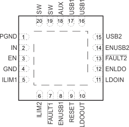
5 Pin Configuration and Functions
RGW Package
20-Pin VQFN With Exposed Thermal Pad
Top View

Pin Functions
| PIN | TYPE(1) | DESCRIPTION | |
|---|---|---|---|
| NAME | NO. | ||
| AUX | 18 | O | Fixed 5.1-V boost converter output. Connect a low-ESR ceramic capacitor from AUX to PGND. |
| EN | 3 | I | Enable input for boost converter. Tie to IN to enable. |
| ENLDO | 12 | I | Enable input for the LDO. Tie to AUX to enable. |
| ENUSB1 | 8 | I | Enable input for the USB1 switch. Tie to IN or AUX to enable. |
| ENUSB2 | 14 | I | Enable input for the USB2 switch. Tie to IN or AUX to enable. |
| FAULT1 | 7 | O | Active low USB1 fault indicator (open drain). |
| FAULT2 | 13 | O | Active low USB2 fault indicator (open drain). |
| GND | 4 | P | Control / logic ground. Must be tied to PGND close to the IC externally. |
| ILIM1 | 5 | I | Program the nominal USB1 switch current-limit threshold with a resistor to GND. |
| ILIM2 | 6 | I | Program the nominal USB2 switch current-limit threshold with a resistor to GND. |
| IN | 2 | I | Input supply voltage for boost converter. |
| LDOIN | 11 | I | Input supply voltage for LDO. Connect to AUX. |
| LDOOUT | 10 | O | Fixed 3.3-V LDO output. Connect a low-ESR ceramic capacitor from LDOOUT to GND. |
| PGND | 1 | P | Source connection for the internal low-side boost converter power switch. Connect to GND with a low impedance connection to the input and output capacitors. |
| RESET | 9 | O | Active low LDO output good indicator (open drain). |
| SW | 19 | P | Boost and rectifying switch input. This node is switched between PGND and AUX. Connect the boost inductor from IN to SW. |
| SW | 20 | P | Boost and rectifying switch input. This node is switched between PGND and AUX. Connect the boost inductor from IN to SW. |
| USB1 | 16 | O | Output of the USB1 power switch. Connect to the USB1 port. |
| USB1 | 17 | O | Output of the USB1 power switch. Connect to the USB1 port. |
| USB2 | 15 | O | Output of the USB2 power switch. Connect to the USB2 port. |
| Thermal Pad | — | — | Internally connected to PGND. Must be soldered to board ground for thermal dissipation. |
(1) I = Input; O = Output; P = Power