SLVSFX8A March 2021 – March 2022 TPS2521
PRODUCTION DATA
- 1 Features
- 2 Applications
- 3 Description
- 4 Revision History
- 5 Device Comparison Table
- 6 Pin Configuration and Functions
- 7 Specifications
-
8 Detailed Description
- 8.1 Overview
- 8.2 Functional Block Diagram
- 8.3
Feature Description
- 8.3.1 Input Reverse Polarity Protection
- 8.3.2 Undervoltage Lockout (UVLO and UVP)
- 8.3.3 Overvoltage Clamp (OVC)
- 8.3.4 Inrush Current, Overcurrent, and Short Circuit Protection
- 8.3.5 Analog Load Current Monitor
- 8.3.6 Reverse Current Protection
- 8.3.7 Overtemperature Protection (OTP)
- 8.3.8 Fault Response
- 8.3.9 Power Good Indication (PG)
- 8.4 Device Functional Modes
- 9 Application and Implementation
- 10Power Supply Recommendations
- 11Layout
- 12Device and Documentation Support
- 13Mechanical, Packaging, and Orderable Information
Package Options
Mechanical Data (Package|Pins)
- RPW|10
Thermal pad, mechanical data (Package|Pins)
Orderable Information
9.3 Typical Application
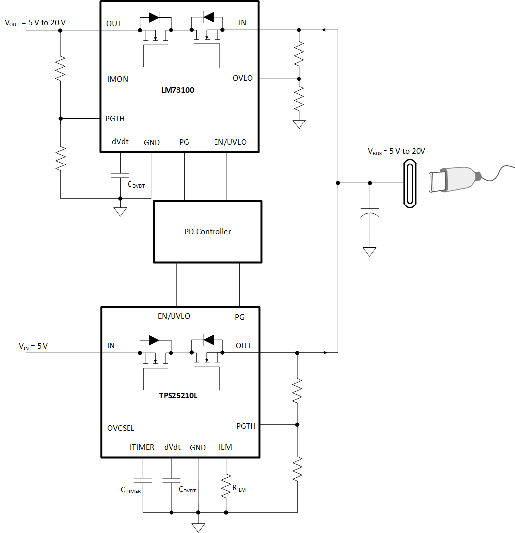
End equipments like PC, notebooks, docking stations, monitors, and so on have USB PD ports which can be configured as DFP (Source), UFP (Sink) or DRP (Source + Sink). TPS2521xx can be used independently or in conjunction with LM73100 to handle the power path protection requirements of USB PD ports as shown in Figure 9-2 below.
TPS2521xx provides overcurrent and short-circuit protection in the source path, while blocking any reverse current from the port to the internal source power rail. The fast recovery (tSWRCB) from reverse current blocking ensures minimum supply droop during Fast Role Swap (FRS) events.
The LM73100 provides overvoltage protection on the sink path, while blocking reverse current from internal sink rail to the port.
The linear ORing mechanism in TPS2521xx and LM73100 ensures that there is no reverse current flowing from one power source to the other during fast or slow ramp of either supply.
 Figure 9-2 USB PD Port Protection