SLVS841F November 2008 – August 2016 TPS2552 , TPS2552-1 , TPS2553 , TPS2553-1
PRODUCTION DATA.
- 1 Features
- 2 Applications
- 3 Description
- 4 Revision History
- 5 Device Comparison Table
- 6 Pin Configuration and Functions
- 7 Specifications
- 8 Parameter Measurement Information
- 9 Detailed Description
- 10Application and Implementation
- 11Power Supply Recommendations
- 12Layout
- 13Device and Documentation Support
- 14Mechanical, Packaging, and Orderable Information
Package Options
Refer to the PDF data sheet for device specific package drawings
Mechanical Data (Package|Pins)
- DBV|6
- DRV|6
Thermal pad, mechanical data (Package|Pins)
- DRV|6
Orderable Information
1 Features
- Up to 1.5-A Maximum Load Current
- ±6% Current-Limit Accuracy at 1.7 A (Typical)
- Meets USB Current-Limiting Requirements
- Backwards Compatible With TPS2550 and TPS2551
- Adjustable Current Limit: 75 mA to 1700 mA (Typical)
- Constant-Current (TPS255x) and Latch-Off (TPS255x-1) Versions
- Fast Overcurrent Response - 2 µs (Typical)
- 85-mΩ High-Side MOSFET (DBV Package)
- Reverse Input-Output Voltage Protection
- Operating Range: 2.5 V to 6.5 V
- Built-In Soft Start
- 15-kV ESD Protection per IEC 61000-4-2 (With External Capacitance)
- UL Listed – File No. E169910 and NEMKO IEC60950-1-am1 ed2.0
- See the TI Switch Portfolio
2 Applications
- USB Ports and Hubs
- Digital TVs
- Set-Top Boxes
- VOIP Phones
3 Description
The TPS255x and TPS255x-1 power-distribution switches are intended for applications where precision current limiting is required or heavy capacitive loads and short circuits are encountered and provide up to 1.5 A of continuous load current. These devices offer a programmable current-limit threshold between 75 mA and 1.7 A (typical) through an external resistor. Current-limit accuracy as tight as ±6% can be achieved at the higher current-limit settings. The power-switch rise and fall times are controlled to minimize current surges during turnon and turnoff.
TPS255x devices limit the output current to a safe level by using a constant-current mode when the output load exceeds the current-limit threshold. TPS255x-1 devices provide circuit breaker functionality by latching off the power switch during overcurrent or reverse-voltage situations. An internal reverse-voltage comparator disables the power-switch when the output voltage is driven higher than the input to protect devices on the input side of the switch. The FAULT output asserts low during overcurrent and reverse-voltage conditions.
Device Information(1)
| PART NUMBER | PACKAGE | BODY SIZE (NOM) |
|---|---|---|
| TPS2552 | SOT-23 (6) | 2.90 mm x 1.60 mm |
| WSON (6) | 2.00 mm x 2.00 mm | |
| TPS2553 | SOT-23 (6) | 2.90 mm x 1.60 mm |
| WSON (6) | 2.00 mm x 2.00 mm |
- For all available packages, see the orderable addendum at the end of the data sheet.
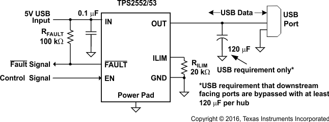
Typical Application
