SLVS841F November   2008  – August 2016 TPS2552 , TPS2552-1 , TPS2553 , TPS2553-1

PRODUCTION DATA.  

  1. Features
  2. Applications
  3. Description
  4. Revision History
  5. Device Comparison Table
  6. Pin Configuration and Functions
  7. Specifications
    1. 7.1 Absolute Maximum Ratings
    2. 7.2 ESD Ratings
    3. 7.3 Recommended Operating Conditions
    4. 7.4 Thermal Information
    5. 7.5 Electrical Characteristics
    6. 7.6 Typical Characteristics
  8. Parameter Measurement Information
  9. Detailed Description
    1. 9.1 Overview
    2. 9.2 Functional Block Diagram
    3. 9.3 Feature Description
      1. 9.3.1 Overcurrent Conditions
      2. 9.3.2 Reverse-Voltage Protection
      3. 9.3.3 FAULT Response
      4. 9.3.4 Undervoltage Lockout (UVLO)
      5. 9.3.5 ENABLE (EN or EN)
      6. 9.3.6 Thermal Sense
    4. 9.4 Device Functional Modes
    5. 9.5 Programming
      1. 9.5.1 Programming the Current-Limit Threshold
  10. 10Application and Implementation
    1. 10.1 Application Information
      1. 10.1.1 Constant-Current vs Latch-Off Operation and Impact on Output Voltage
    2. 10.2 Typical Applications
      1. 10.2.1 Two-Level Current-Limit Circuit
        1. 10.2.1.1 Design Requirements
        2. 10.2.1.2 Detailed Design Procedures
          1. 10.2.1.2.1 Designing Above a Minimum Current Limit
          2. 10.2.1.2.2 Designing Below a Maximum Current Limit
          3. 10.2.1.2.3 Accounting for Resistor Tolerance
          4. 10.2.1.2.4 Input and Output Capacitance
        3. 10.2.1.3 Application Curves
      2. 10.2.2 Auto-Retry Functionality
        1. 10.2.2.1 Design Requirements
        2. 10.2.2.2 Detailed Design Procedure
      3. 10.2.3 Typical Application as USB Power Switch
        1. 10.2.3.1 Design Requirements
          1. 10.2.3.1.1 USB Power-Distribution Requirements
        2. 10.2.3.2 Detailed Design Procedure
          1. 10.2.3.2.1 Universal Serial Bus (USB) Power-Distribution Requirements
  11. 11Power Supply Recommendations
    1. 11.1 Self-Powered and Bus-Powered Hubs
    2. 11.2 Low-Power Bus-Powered and High-Power Bus-Powered Functions
    3. 11.3 Power Dissipation and Junction Temperature
  12. 12Layout
    1. 12.1 Layout Guidelines
    2. 12.2 Layout Example
  13. 13Device and Documentation Support
    1. 13.1 Device Support
    2. 13.2 Related Links
    3. 13.3 Receiving Notification of Documentation Updates
    4. 13.4 Community Resources
    5. 13.5 Trademarks
    6. 13.6 Electrostatic Discharge Caution
    7. 13.7 Glossary
  14. 14Mechanical, Packaging, and Orderable Information

Package Options

Refer to the PDF data sheet for device specific package drawings

Mechanical Data (Package|Pins)
  • DBV|6
  • DRV|6
Thermal pad, mechanical data (Package|Pins)
Orderable Information

12 Layout

12.1 Layout Guidelines

  • TI recommends placing the 100-nF bypass capacitor near the IN and GND pins, and make the connections using a low-inductance trace.
  • TI recommends placing a high-value electrolytic capacitor and a 100-nF bypass capacitor on the output pin when large transient currents are expected on the output.
  • The traces routing the RILIM resistor to the device must be as short as possible to reduce parasitic effects on the current limit accuracy.
  • The PowerPAD must be directly connected to PCB ground plane using wide and short copper trace.

12.2 Layout Example
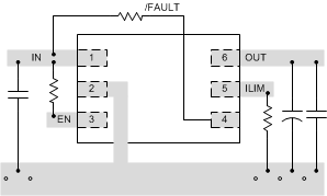
TPS2552 TPS2553 TPS2552-1 TPS2553-1 layout_slvs841.gif Figure 30. Layout Recommendation