SLVSFP2B November 2020 – September 2021 TPS25864-Q1 , TPS25865-Q1
PRODUCTION DATA
- 1 Features
- 2 Applications
- 3 Description
- 4 Revision History
- 5 Description (continued)
- 6 Device Comparison Table
- 7 Pin Configuration and Functions
- 8 Specifications
- 9 Parameter Measurement Information
-
10Detailed Description
- 10.1 Overview
- 10.2 Functional Block Diagram
- 10.3
Feature Description
- 10.3.1 Power-Down or Undervoltage Lockout
- 10.3.2 Input Overvoltage Protection (OVP) - Continuously Monitored
- 10.3.3 Buck Converter
- 10.3.4 FREQ/SYNC
- 10.3.5 Bootstrap Voltage (BOOT)
- 10.3.6 Minimum ON-Time, Minimum OFF-Time
- 10.3.7 Internal Compensation
- 10.3.8 Selectable Output Voltage (VSET)
- 10.3.9 Current Limit and Short Circuit Protection
- 10.3.10 Cable Compensation
- 10.3.11 Thermal Management With Temperature Sensing (TS) and OTSD
- 10.3.12 Thermal Shutdown
- 10.3.13 USB Specification Overview
- 10.3.14 USB Port Operating Modes
- 10.4 Device Functional Modes
- 11Application and Implementation
- 12Power Supply Recommendations
- 13Layout
- 14Device and Documentation Support
- 15Mechanical, Packaging, and Orderable Information
Package Options
Mechanical Data (Package|Pins)
- RPQ|25
Thermal pad, mechanical data (Package|Pins)
Orderable Information
7 Pin Configuration and Functions
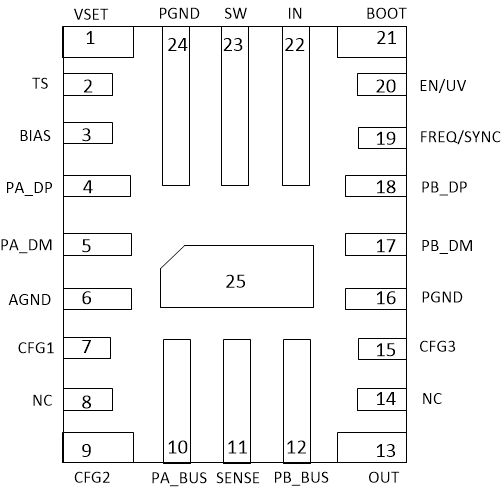
 Figure 7-1 TPS2586x-Q1 RPQ Package25-Pin
(QFN)Top View
Figure 7-1 TPS2586x-Q1 RPQ Package25-Pin
(QFN)Top ViewTable 7-1 Pin Functions for TPS2586x-Q1 RPQ
Package
| PIN | TYPE (1) | DESCRIPTION | |
|---|---|---|---|
| NAME | NO. | ||
| VSET | 1 | A | Output Voltage Setting. Short to GND to set the 5.17-V output voltage. Float or pull up to VSENSE to set 5.1-V output voltage. Tie to GND through a 40.2-KΩ resistor to set 5.3-V output voltage. Tie to GND through a 80.6-KΩ resistor to set 5.4-V output voltage. |
| TS | 2 | A | Temperature Sense terminal. Connect the TS input to the NTC thermistor. |
| BIAS | 3 | P | Input of internal bias supply. Must connect to the SENSE pin directly. Power the internal circuit. |
| PA_DP | 4 | A | D+ data line. Connect to USB Port A connector. |
| PA_DM | 5 | A | D- data line. Connect to USB Port A connector. |
| AGND | 6 | P | Analog ground terminal. Connect AGND to PGND. |
| CFG1 | 7 | A | Configuration pin. For internal circuit, must connect a 5.1-KΩ resistor to AGND. |
| NC | 8, 14 | A | Makes no electrical connection. |
| CFG2 | 9 | A | Configuration pin. For internal circuit, must connect a 11.8-KΩ resistor to AGND. |
| PA_BUS | 10 | P | Port A BUS output. |
| SENSE | 11 | P | Output Voltage Sensing. External load on this pin is strictly prohibited. Connect to the other side of the external inductor. |
| PB_BUS | 12 | P | Port B BUS output. |
| OUT | 13 | P | Output pin. Provide 5.1-V voltage to power external load with maximum 200-mA capability. The voltage follows the VSET setting. |
| CFG3 | 15 | A | Configuration pin. For internal circuit, must connect a 5.1-KΩ resistor to AGND. |
| PGND | 16, 24, 25 | P | Power Ground terminal. Connected to the source of LS FET internally. Connect to system ground, AGND, and the ground side of the CIN and COUT capacitors. The path to CIN must be as short as possible. |
| PB_DM | 17 | A | D- data line. Connect to USB port B connector. |
| PB_DP | 18 | A | D+ data line. Connect to USB port B connector. |
| FREQ/ SYNC | 19 | A | Switching Frequency Program and External Clock Input. Connect a resistor from FREQ to GND to set the switching frequency. |
| EN/UV | 20 | A | Enable pin. Precision enable controls the regulator switching action. Do not float. High = on, Low = off. Can be tied to SENSE directly. Precision enable input allows adjustable UVLO by external resistor divider if tie to IN pin. |
| BOOT | 21 | P | Bootstrap capacitor connection. Internally, the BOOT is connected to the cathode of the boost-strap diode. Connect the 0.1-μF bootstrap capacitor from SW to BOOT. |
| IN | 22 | P | Input power. Connected to external DC supply. Expected range of bypass capacitors is 1 μF to 10 μF, connect from IN to PGND. Can withstand up to 36 V without damage but operating is suspended if VIN is above the 26-V OVP threshold. |
| SW | 23 | P | Switching output of the regulator. Internally connected to source of the HS FET and drain of the LS FET. Connect to output inductor. |
(1) A = Analog, P = Power, G = Ground.