SLVSFP2B November 2020 – September 2021 TPS25864-Q1 , TPS25865-Q1
PRODUCTION DATA
- 1 Features
- 2 Applications
- 3 Description
- 4 Revision History
- 5 Description (continued)
- 6 Device Comparison Table
- 7 Pin Configuration and Functions
- 8 Specifications
- 9 Parameter Measurement Information
-
10Detailed Description
- 10.1 Overview
- 10.2 Functional Block Diagram
- 10.3
Feature Description
- 10.3.1 Power-Down or Undervoltage Lockout
- 10.3.2 Input Overvoltage Protection (OVP) - Continuously Monitored
- 10.3.3 Buck Converter
- 10.3.4 FREQ/SYNC
- 10.3.5 Bootstrap Voltage (BOOT)
- 10.3.6 Minimum ON-Time, Minimum OFF-Time
- 10.3.7 Internal Compensation
- 10.3.8 Selectable Output Voltage (VSET)
- 10.3.9 Current Limit and Short Circuit Protection
- 10.3.10 Cable Compensation
- 10.3.11 Thermal Management With Temperature Sensing (TS) and OTSD
- 10.3.12 Thermal Shutdown
- 10.3.13 USB Specification Overview
- 10.3.14 USB Port Operating Modes
- 10.4 Device Functional Modes
- 11Application and Implementation
- 12Power Supply Recommendations
- 13Layout
- 14Device and Documentation Support
- 15Mechanical, Packaging, and Orderable Information
Package Options
Mechanical Data (Package|Pins)
- RPQ|25
Thermal pad, mechanical data (Package|Pins)
Orderable Information
10.3.4 FREQ/SYNC
The switching frequency of the TPS2586x-Q1 can be programmed by the resistor, RFREQ, from the FREQ/SYNC pin and AGND pin. To determine the FREQ resistance for a given switching frequency, use Equation 4:
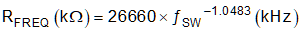
 Figure 10-3 FREQ Set Resistor vs Switching
Frequency
Figure 10-3 FREQ Set Resistor vs Switching
FrequencyThe normal method of setting the buck regulator switching frequency is by selecting an appropriate value FREQ resistor. The typical FREQ resistors value are listed in Table 10-1. Please note that TPS25865-Q1 can only support frequency up to 800 kHz.
| FREQ (KΩ) | SWITCHING FREQUENCY (KHz) |
|---|---|
| 80.6 | 253 |
| 49.9 | 400 |
| 19.1 | 1000 |
| 8.87 | 2100 |
| 8.45 | 2200 |
The FREQ/SYNC pin can be used to synchronize the internal oscillator to an external clock. The internal oscillator can be synchronized by AC coupling a positive edge into the FREQ/SYNC pin. When using a low impedance signal source, the frequency setting resistor, FREQ, is connected in parallel with an AC coupling capacitor, CCOUP, to a termination resistor, RTERM (for example, 50 Ω). The two resistors in series provide the default frequency setting resistance when the signal source is turned off. A 10-pF ceramic capacitor can be used for CCOUP. The AC coupled peak-to-peak voltage at the FREQ/SYNC pin must exceed the SYNC amplitude threshold of 1.2 V (typical) to trip the internal synchronization pulse detector, and the minimum SYNC clock HIGH and LOW time must be longer than 100 ns (typical). A 2.5 V or higher amplitude pulse signal coupled through a 1-nF capacitor, CSYNC, is a good starting point. Figure 10-4 shows the device synchronized to an external system clock. The external clock must be off before startup to allow proper startup sequencing.
 Figure 10-4 Synchronize to External Clock
TPS25864-Q1 switching action can be synchronized to an external clock from 200 KHz to 3 MHz. TPS25865-Q1 switching action can be synchronized to an external clock from 200 KHz to 800 kHz. Note the higher switching frequency results in more power loss on IC, causing the junction temperature and also the board temperature rising. Then, the device can enter load shedding under high ambient temperature.