SLVSCE1C August 2014 – November 2015 TPS25921A , TPS25921L
PRODUCTION DATA.
- 1 Features
- 2 Applications
- 3 Description
- 4 Application Schematic
- 5 Revision History
- 6 Pin Configuration and Functions
- 7 Specifications
- 8 Parametric Measurement Information
-
9 Detailed Description
- 9.1 Overview
- 9.2 Functional Block Diagram
- 9.3 Feature Description
- 9.4 Device Functional Modes
-
10Applications and Implementation
- 10.1 Application Information
- 10.2
Typical Application
- 10.2.1
Precision Current Limiting and Protection for White Goods
- 10.2.1.1 Design Requirements
- 10.2.1.2 Detailed Design Procedure
- 10.2.1.3 Application Curves
- 10.2.1
Precision Current Limiting and Protection for White Goods
- 10.3 System Examples
- 11Power Supply Recommendations
- 12Layout
- 13Device and Documentation Support
- 14Mechanical, Packaging, and Orderable Information
Package Options
Mechanical Data (Package|Pins)
- D|8
Thermal pad, mechanical data (Package|Pins)
Orderable Information
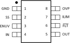
6 Pin Configuration and Functions
D Package
8-Pin SOIC
Top View

Pin Functions
| NAME | NUMBER | DESCRIPTION |
|---|---|---|
| GND | 1 | Ground. |
| SS | 2 | A capacitor from this pin to GND sets the ramp rate of output voltage at device turn-on. |
| ENUV | 3 | Input for setting programmable undervoltage lockout threshold. An undervoltage event will open internal FET and assert FLT to indicate power-failure. When pulled to GND, resets the thermal fault latch in TPS25921L. |
| IN | 4 | Power Input and supply voltage of the device. |
| OUT | 5 | Power Output of the device. |
| FLT | 6 | Fault event indicator, goes low to indicate fault condition due to Undervoltage, Overvoltage, and Thermal shutdown event. A nuisance fast trip does not trigger fault. It is an open drain output. |
| ILIM | 7 | A resistor from this pin to GND will set the overload and short circuit limit. |
| OVP | 8 | Input for setting programmable overvoltage protection threshold. An overvoltage event will open the internal FET and assert FLT to indicate overvoltage. |