SLVSDJ0E May 2016 – January 2021 TPS25940-Q1
PRODMIX
- 1 Features
- 2 Applications
- 3 Description
- 4 Revision History
- 5 Device Comparison Table
- 6 Pin Configuration and Functions
- 7 Specifications
- 8 Parametric Measurement Information
-
9 Detailed Description
- 9.1 Overview
- 9.2 Functional Block Diagram
- 9.3 Feature Description
- 9.4 Device Functional Modes
-
10Application and Implementation
- 10.1 Application Information
- 10.2
Typical Application
- 10.2.1 Design Requirements
- 10.2.2
Detailed Design Procedure
- 10.2.2.1 Step by Step Design Procedure
- 10.2.2.2 Programming the Current-Limit Threshold: R(ILIM) Selection
- 10.2.2.3 Undervoltage Lockout and Overvoltage Set Point
- 10.2.2.4 Programming Current Monitoring Resistor—RIMON
- 10.2.2.5 Setting Output Voltage Ramp Time (tdVdT)
- 10.2.2.6 Programing the Power Good Set Point
- 10.2.2.7 Support Component Selections—R6, R7 and CIN
- 10.2.3 Application Curves
- 10.2.4 System Examples
- 11Power Supply Recommendations
- 12Layout
- 13Device and Documentation Support
- 14Mechanical, Packaging, and Orderable Information
Package Options
Mechanical Data (Package|Pins)
- RVC|20
Thermal pad, mechanical data (Package|Pins)
- RVC|20
Orderable Information
3 Description
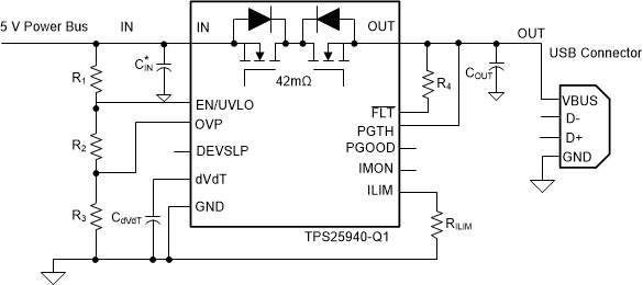
The TPS25940xx-Q1 eFuse Power Switches are compact, feature rich power management devices with a full suite of protection functions. The wide operating range allows control of many popular DC bus voltages. Integrated back-to-back FETs provide bidirectional current control making the device well suited for systems with load side holdup energy that must not drain back to a failed supply bus.
Load, source and device protection are provided with many programmable features including overcurrent, dVo/dt ramp and overvoltage, undervoltage thresholds. For system status monitoring and downstream load control, the device provides PGOOD, FLT and precise current monitor output. Precise programmable undervoltage, overvoltage thresholds and mode simplify power management design.
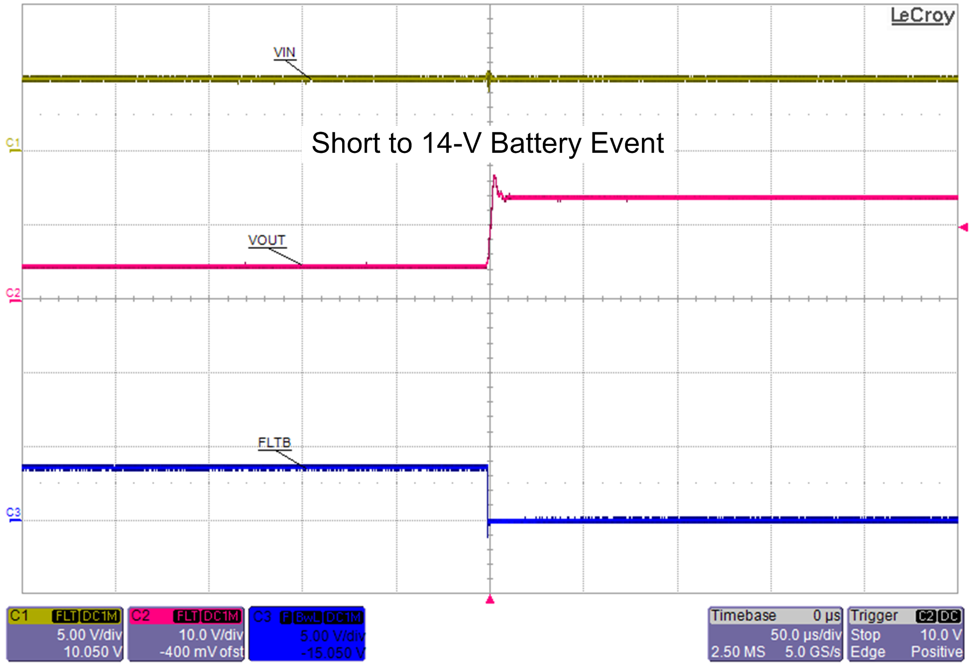
The TPS25940xx-Q1 monitor V(IN) and V(OUT) to provide true reverse current blocking when V(IN) < (V(OUT) – 66 mV). This function supports supply bus protection from over-voltages during output short to battery faults.
| PART NUMBER | PACKAGE | BODY SIZE (NOM) |
|---|---|---|
| TPS25940-Q1 | WQFN (20) | 3.00 mm x 4.00 mm |
| TPS25940L-Q1 | ||
| TPS259401A-Q1 |
 Simplified Schematic
 Output Short-to-Battery
Detection and Protection