SLVSCE9D June 2014 – October 2017 TPS25942A , TPS25942L , TPS25944A , TPS25944L
UNLESS OTHERWISE NOTED, this document contains PRODUCTION DATA.
- 1 Features
- 2 Applications
- 3 Description
- 4 Revision History
- 5 Device Comparison Table
- 6 Pin Configuration and Functions
- 7 Specifications
- 8 Parameter Measurement Information
-
9 Detailed Description
- 9.1 Overview
- 9.2 Functional Block Diagram
- 9.3
Feature Description
- 9.3.1 Enable and Adjusting Undervoltage Lockout
- 9.3.2 Overvoltage Protection (OVP)
- 9.3.3 Hot Plug-In and In-Rush Current Control
- 9.3.4 Overload and Short Circuit Protection
- 9.3.5 Reverse Current Protection
- 9.3.6 FAULT Response
- 9.3.7 Current Monitoring
- 9.3.8 Power Good Comparator
- 9.3.9 IN, OUT and GND Pins
- 9.3.10 Thermal Shutdown
- 9.4 Device Functional Modes
-
10Application and Implementation
- 10.1 Application Information
- 10.2
Typical Application
- 10.2.1 Design Requirements
- 10.2.2
Detailed Design Procedure
- 10.2.2.1 Step by Step Design Procedure
- 10.2.2.2 Programming the Current-Limit Threshold: R(ILIM) Selection
- 10.2.2.3 Undervoltage Lockout and Overvoltage Set Point
- 10.2.2.4 Programming Current Monitoring Resistor—RIMON
- 10.2.2.5 Setting Output Voltage Ramp Time (tdVdT)
- 10.2.2.6 Programing the Power Good Set Point
- 10.2.2.7 Support Component Selections—R6, R7 and CIN
- 10.2.3 Application Curves
- 10.3 System Examples
- 11Power Supply Recommendations
- 12Layout
- 13Device and Documentation Support
- 14Mechanical, Packaging, and Orderable Information
Package Options
Mechanical Data (Package|Pins)
- RVC|20
Thermal pad, mechanical data (Package|Pins)
- RVC|20
Orderable Information
10.3.1.2 Priority Power MUX Operation
Applications having two energy sources such as PCIe cards, Tablets and Portable battery powered equipment require preference of one source to another. For example, mains power (wall-adapter) has the priority over the internal back-up power or auxiliary power. These applications demand for switch over from mains power to back-up power only when main input voltage falls below a user defined threshold. The devices provide a simple solution for priority power multiplexing needs.
Figure 79 shows a typical priority power multiplexing implementation using devices. When primary power IN1 is present, the device in IN1 path powers the OUT bus irrespective of whether auxiliary power IN2 is greater than or less than IN1. Once the voltage on the IN1 rail falls below the user-defined threshold, the device IN1 issues a signal to switch over to auxiliary power IN2. The transition happens seamlessly in less than 125 µs, with minimal voltage droop on the bus. The voltage droop during transition is a function of load current and bus capacitance (see Equation 36).

where
- V(droop) in Volts, I(Load) is load current in Ampere, C(BUS) is bus capacitance in µF
When the main voltage supply (IN1) is not present or during brown-out conditions, the device in auxiliary supply rail (IN2) provides power to the output. When IN1 recovers, the device connected to IN1 is turned on at defined slew rate and the device in IN2 path is turned off, allowing a seamless transition from auxiliary to the main voltage supply with minimal droop and with no shoot-through current.
Priority power multiplexing can be done either between two similar rails (such as 12 V Primary to 12 V Aux, 3.3 V Primary to 3.3 V Aux) or between dissimilar rails (such as 12 V Primary to 5 V Aux or 3.3 V Aux; or vice versa).
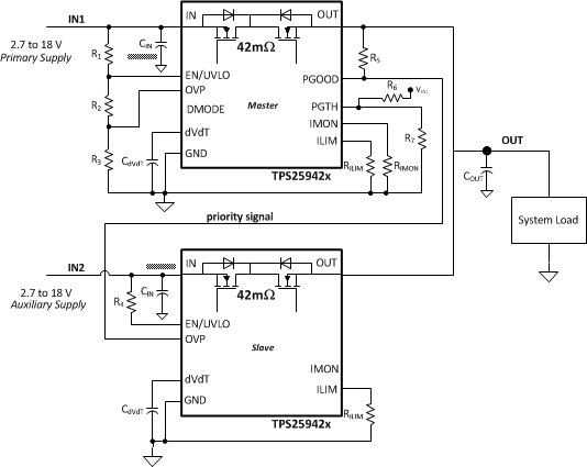
Figure 80 and Figure 81 show typical switch-over waveforms of Priority Muxing implementation using the TPS25942 or TPS25944 for 11.5 V Primary and 14.5 V Auxiliary Bus.
Figure 82 and Figure 83 show typical switch-over waveforms of Priority Muxing implementation using the TPS25942 or TPS25944 for 12 V Primary and 3.3 V Auxiliary Bus.
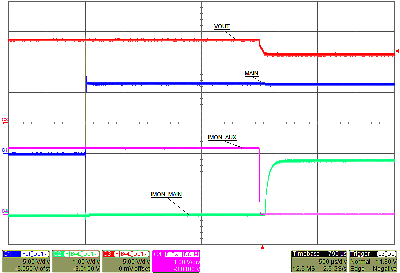
| V(IN1) = 11.5 V | R(ILIM1) = 24.6 kΩ, | C(OUT) = 150 µF |
| V(IN2) = 14.5 V | R(ILIM2) = 33.2 kΩ | C(dVdT) = 1.2 nF |
| RL = 5.6 Ω | R(IMON) = 16.2 kΩ | V(UVLO-High) = 10.8 V |
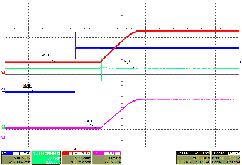
| V(IN1) = 12 V | R(ILIM1) = 24.6 kΩ | C(OUT) = 150 µF |
| V(IN2) = 3.3 V | R(ILIM2) = 33.2 kΩ | C(dVdT) = 1.2 nF |
| RLoad = 5.6 Ω | R(IMON) = 16.2 kΩ | V(UVLO-High) = 10.8 V |
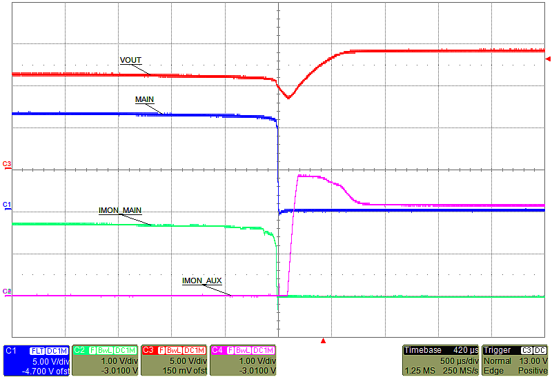
| V(IN1) = 11.5 V | R(ILIM1) = 24.6 kΩ | C(OUT) = 150 µF |
| V(IN2) = 14.5 V | R(ILIM2) = 33.2 kΩ | C(dVdT) = 1.2 nF |
| RL = 5.6 Ω | R(IMON) = 16.2 kΩ | V(UVLO-Low) = 10.2 V |
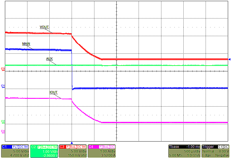
| V(IN1) = 12 V | R(ILIM1) = 24.6 kΩ | C(OUT) = 150 µF |
| V(IN2) = 3.3 V | R(ILIM2) = 33.2 kΩ | C(dVdT) = 1.2 nF |
| RL = 5.6 Ω | R(IMON) = 16.2 kΩ | V(UVLO-Low) = 10.2 V |