SLVSCE9D June 2014 – October 2017 TPS25942A , TPS25942L , TPS25944A , TPS25944L
UNLESS OTHERWISE NOTED, this document contains PRODUCTION DATA.
- 1 Features
- 2 Applications
- 3 Description
- 4 Revision History
- 5 Device Comparison Table
- 6 Pin Configuration and Functions
- 7 Specifications
- 8 Parameter Measurement Information
-
9 Detailed Description
- 9.1 Overview
- 9.2 Functional Block Diagram
- 9.3
Feature Description
- 9.3.1 Enable and Adjusting Undervoltage Lockout
- 9.3.2 Overvoltage Protection (OVP)
- 9.3.3 Hot Plug-In and In-Rush Current Control
- 9.3.4 Overload and Short Circuit Protection
- 9.3.5 Reverse Current Protection
- 9.3.6 FAULT Response
- 9.3.7 Current Monitoring
- 9.3.8 Power Good Comparator
- 9.3.9 IN, OUT and GND Pins
- 9.3.10 Thermal Shutdown
- 9.4 Device Functional Modes
-
10Application and Implementation
- 10.1 Application Information
- 10.2
Typical Application
- 10.2.1 Design Requirements
- 10.2.2
Detailed Design Procedure
- 10.2.2.1 Step by Step Design Procedure
- 10.2.2.2 Programming the Current-Limit Threshold: R(ILIM) Selection
- 10.2.2.3 Undervoltage Lockout and Overvoltage Set Point
- 10.2.2.4 Programming Current Monitoring Resistor—RIMON
- 10.2.2.5 Setting Output Voltage Ramp Time (tdVdT)
- 10.2.2.6 Programing the Power Good Set Point
- 10.2.2.7 Support Component Selections—R6, R7 and CIN
- 10.2.3 Application Curves
- 10.3 System Examples
- 11Power Supply Recommendations
- 12Layout
- 13Device and Documentation Support
- 14Mechanical, Packaging, and Orderable Information
Package Options
Mechanical Data (Package|Pins)
- RVC|20
Thermal pad, mechanical data (Package|Pins)
- RVC|20
Orderable Information
7.7 Typical Characteristics
Conditions are –40°C ≤ TJ = TA ≤ +125°C, V(IN) = 12 V, V(EN/UVLO) = 2 V, V(OVP) = V(DMODE) = V(PGTH) = 0 V, R(ILIM) = 150 kΩ, C(OUT) = 1 µF, C(dVdT) = OPEN, PGOOD = FLT = IMON = OPEN. (unless stated otherwise)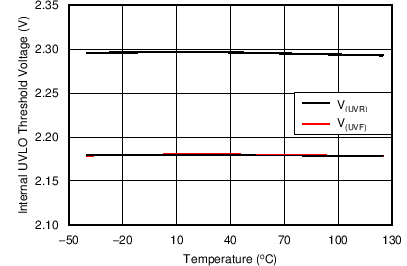
Figure 1. Internal UVLO Threshold Voltage vs Temperature
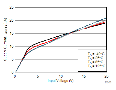
Figure 3. Input Supply Current vs Supply Voltage at Shutdown
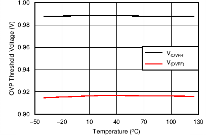
Figure 5. OVP Threshold Voltage vs Temperature
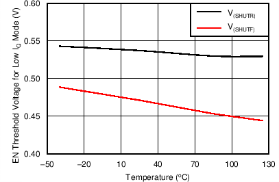
Figure 7. EN Threshold Voltage for Low IQ Mode vs Temperature
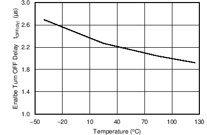
Figure 9. Enable Turnoff Delay vs Temperature
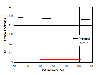
Figure 11. DMODE Threshold Voltage vs Temperature
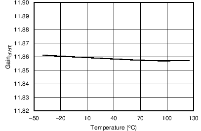
Figure 13. GAIN(dVdT) vs Temperature
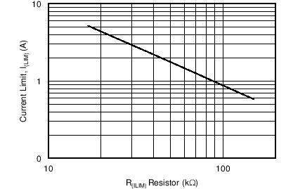
Figure 15. Current Limit vs Current Limit Resistor
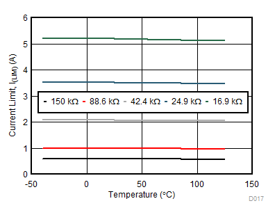
Figure 17. Current Limit vs Temperature Across R(ILIM)
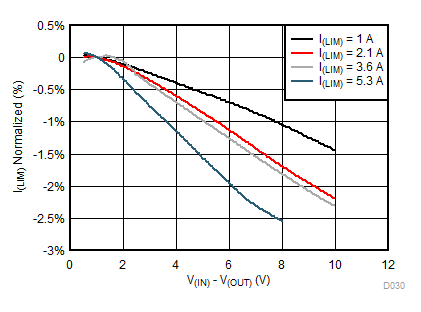
| For I(LIM) = 5.3 A, device goes into thermal shutdown for | ||
| [V(IN) – V(OUT)] > 8 V |
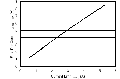
Figure 21. Fast Trip Threshold vs Current Limit
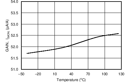
Figure 23. GAIN(IMON) vs Temperature
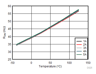
Figure 25. RON vs Temperature Across Load Current
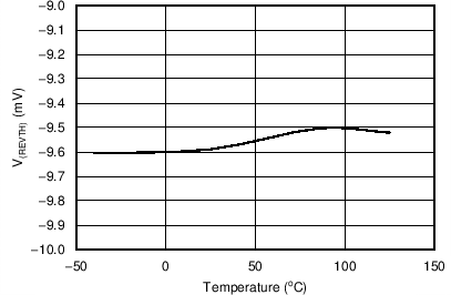
Figure 27. V(REVTH) vs Temperature
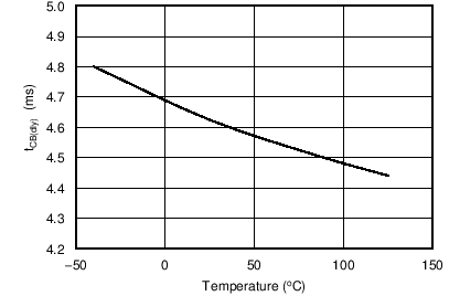
Figure 29. Circuit Breaker Timer Fault Assertion Delay vs Temperature
| V(IN) = 4.5 V |
.png)
| R(FLT) = 100 kΩ |
.png)
| V(IN) = 12 V | RL = 12 Ω | R(FLT) = 100 kΩ |
| V(IN) = 12 V | RL = 12 Ω | R(FLT) = 100 kΩ |
| R(PGOOD) = 100 kΩ |
| V(IN) = 12 V | R(IMON) = 16.9 kΩ | R(FLT) = 100 kΩ |
| R(ILIM) = 17.8 KΩ |
.png)
Figure 41. Transition from Normal Mode to Non-Ideal Diode Mode
| V(IN) = 12 V | RL = 3 Ω to 2 Ω | R(IMON) = 16.9 kΩ |
| R(ILIM) = 17.8 KΩ | R(FLT) = 100 kΩ |
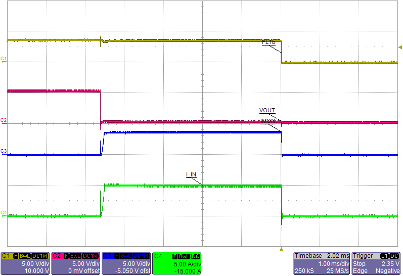
| V(IN) = 5 V | R(IMON) = 16.9 kΩ | R(FLT) = 100 kΩ |
| R(ILIM) = 17.8 KΩ |
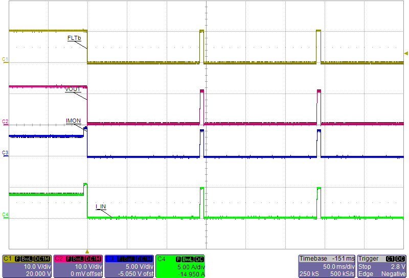
Device Turns Off after the Fault Timer tCB(dly) (4 ms) Expires
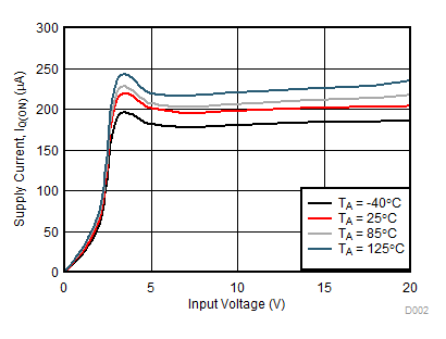
Figure 2. Input Supply Current vs Supply Voltage During Normal Operation
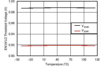
Figure 4. EN Threshold Voltage vs Temperature
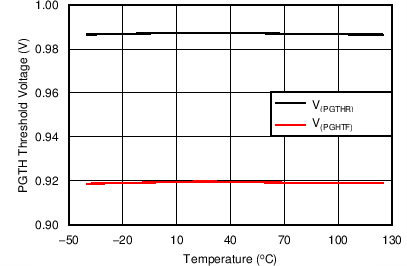
Figure 6. PGTH Threshold Voltage vs Temperature
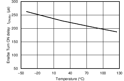
Figure 8. Enable Turnon Delay vs Temperature
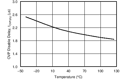
Figure 10. OVP Disable Delay vs Temperature
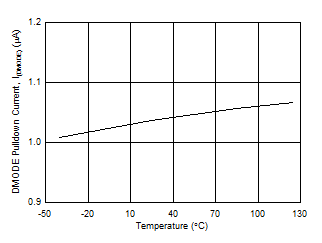
Figure 12. DMODE Pulldown Current vs Temperature
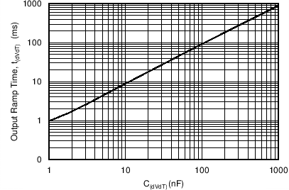
Figure 14. Output Ramp Time vs C(dVdT)
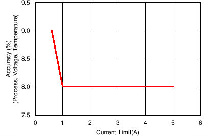
Figure 16. Current Limit Accuracy vs Current Limit
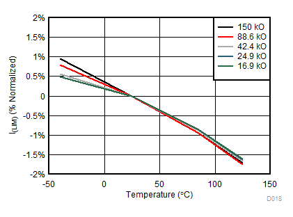
Figure 18. Current Limit (% Normalized) vs Temperature
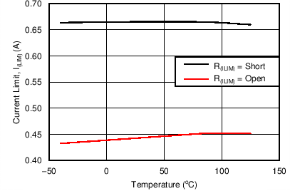
Figure 20. Current Limit for R(ILIM) = Open and Short vs Temperature
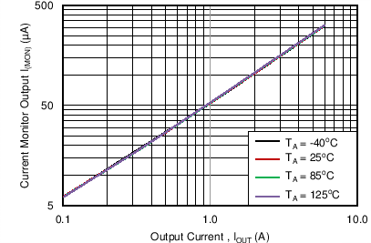
Figure 24. Current Monitor Output vs Output Current
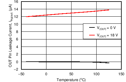
Figure 26. OUT Leakage Current in Off State vs Temperature
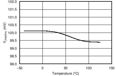
Figure 28. V(FWDTH) vs Temperature
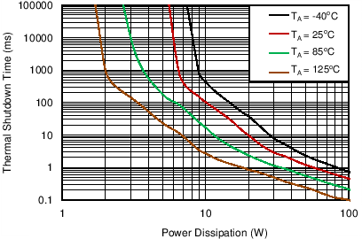
| Taken on 2-Layer board, 2oz.(0.08-mm thick) with GND plane area: 14 cm2 (Top) and 20 cm2 (Bottom) |
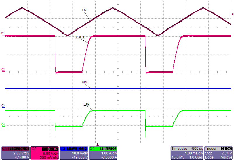
| V(IN) = 11 V |
.png)
| R(FLT) = 100 kΩ |
.png)
| V(IN) = 12 V | RL = 12 Ω | R(FLT) = 100 kΩ |
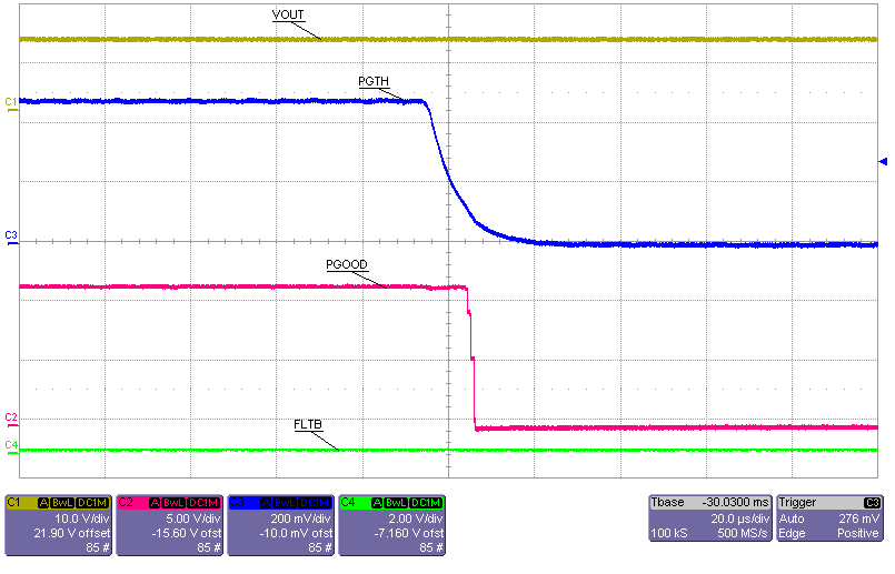
| V(IN) = 12 V | RL = 12 Ω | R(FLT) = 100 kΩ |
| R(PGOOD) = 100 kΩ |
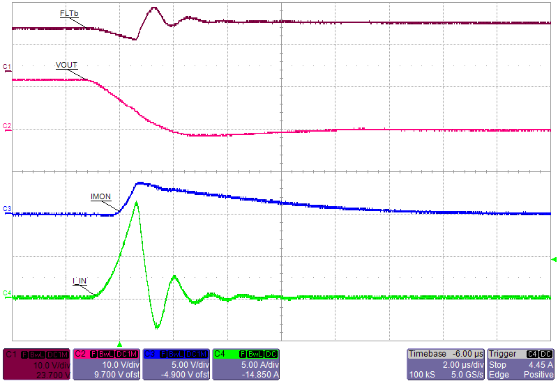
| V(IN) = 12 V | R(IMON) = 16.9 kΩ | R(FLT) = 100 kΩ |
| R(ILIM) = 17.8 KΩ |
.png)
Figure 42. Transition from Non-Ideal Diode Mode to Normal Mode
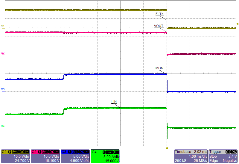
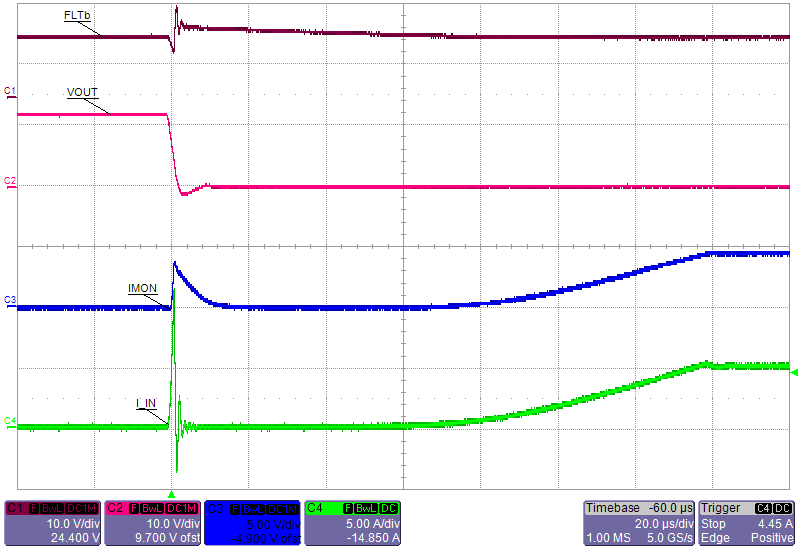
Figure 44. Overload: Zoomed In (First Cycle)
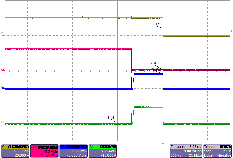
| V(IN) = 12 V | R(IMON) = 16.9 kΩ | R(FLT) = 100 kΩ | ||
| R(ILIM) = 17.8 KΩ |
Device Turns Off When TJ > T(TSD) Before Timer Expires
