SLVSBR5C December 2012 – June 2015 TPS27082L
PRODUCTION DATA.
- 1 Features
- 2 Applications
- 3 Description
- 4 Revision History
- 5 Pin Configuration and Functions
- 6 Specifications
- 7 Detailed Description
-
8 Application and Implementation
- 8.1 Application Information
- 8.2 Typical Application
- 8.3
System Examples
- 8.3.1 TFT LCD Module Inrush Current Control
- 8.3.2 Standby Power Isolation
- 8.3.3 Boost Regulator With True Shutdown
- 8.3.4 Single Module Multiple Power Supply Sequencing
- 8.3.5 Multiple Modules Interdependent Power Supply Sequencing
- 8.3.6 Multiple Modules Interdependent Supply Sequencing Without a GPIO Input
- 9 Power Supply Recommendations
- 10Layout
- 11Device and Documentation Support
- 12Mechanical, Packaging, and Orderable Information
Package Options
Mechanical Data (Package|Pins)
- DDC|6
Thermal pad, mechanical data (Package|Pins)
Orderable Information
5 Pin Configuration and Functions
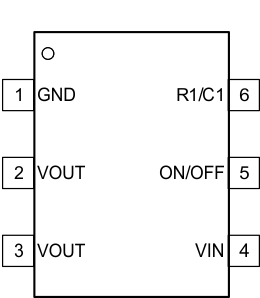
DDC Package
6-Pin SOT
Top View

Pin Functions
| PIN | I/O | DESCRIPTION | |
|---|---|---|---|
| NAME | NO. | ||
| GND | 1 | I | Connect to the system GND |
| VOUT | 2 | O | Drain Terminal of Power PFET (Q1) – If required, connect a slew control capacitor between pins VOUT and R1/C |
| 3 | |||
| VIN | 4 | I | Source Terminal of Power PFET (Q1) – connect a pull-up resistor between the pins VIN and R1/C1 |
| ON/OFF | 5 | I | Active high enable – when driven with a high impedance driver, connect an external pull down resistor to GND |
| R1/C1 | 6 | I | Gate Terminal of Power PFET (Q1) |