SLVSCI7C March 2014 – March 2021 TPS3700-Q1
PRODUCTION DATA
- 1 Features
- 2 Applications
- 3 Description
- 4 Revision History
- 5 Pin Configuration and Functions
- 6 Specifications
- 7 Detailed Description
- 8 Application and Implementation
- 9 Power Supply Recommendations
- 10Layout
- 11Device and Documentation Support
- 12Mechanical, Packaging, and Orderable Information
Package Options
Mechanical Data (Package|Pins)
Thermal pad, mechanical data (Package|Pins)
Orderable Information
3 Description
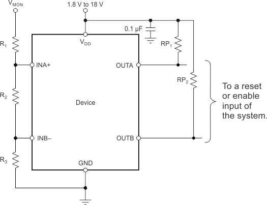
The TPS3700-Q1 wide-supply window voltage detector operates over a 1.8 V to 18 V range. The device has two high-accuracy comparators with an internal 400-mV reference and two open-drain outputs rated to 18 V for overvoltage and undervoltage detection. The TPS3700-Q1 device can be used as a window voltage detector or as two independent voltage monitors; the monitored voltage can be set with the use of external resistors. For even wider input voltage capability up to 65 V, see the TPS37A-Q1 or the TPS38A-Q1 devices.
The OUTA terminal is driven low when the voltage at the INA+ terminal drops below (VIT+ – Vhys), and goes high when the voltage returns above the respective threshold (VIT+). The OUTB terminal is driven low when the voltage at the INB– terminal rises above VIT+, and goes high when the voltage drops below the respective threshold (VIT+ – Vhys). Both comparators in the TPS3700-Q1 device include built-in hysteresis for filtering to reject brief glitches, thereby ensuring stable output operation without false triggering.
The TPS3700-Q1 device is available in a Thin SOT-6 and a 1.5-mm x 1.5-mm WSON-6 package and is specified over the junction temperature range of –40°C to 125°C.
| ORDER NUMBER | PACKAGE (1) | BODY SIZE |
|---|---|---|
| TPS3700-Q1 | SOT23 (6) | 2.90 mm × 1.60 mm |
| WSON (6) | 1.50 mm x 1.50 mm |
 Simplified Schematic
 Output vs Input Thresholds and
Hysteresis