SBVS272B November   2015  – December 2023 TPS3711

PRODUCTION DATA  

  1.   1
  2. Features
  3. Applications
  4. Description
  5. Pin Configuration and Functions
  6. Specifications
    1. 5.1 Absolute Maximum Ratings #GUID-795AD25B-5DDA-4725-83BA-87F5B93DF96A/ABSMAXNOTE
    2. 5.2 ESD Ratings
    3. 5.3 Recommended Operating Conditions
    4. 5.4 Thermal Information
    5. 5.5 Electrical Characteristics
    6. 5.6 Timing Requirements
    7. 5.7 Typical Characteristics
  7. Detailed Description
    1. 6.1 Overview
    2. 6.2 Functional Block Diagram
    3. 6.3 Feature Description
      1. 6.3.1 Input Pin (SENSE)
      2. 6.3.2 Output Pin (OUT)
    4. 6.4 Device Functional Modes
      1. 6.4.1 Normal Operation (VDD > UVLO)
      2. 6.4.2 Undervoltage Lockout (V(POR) < VDD < UVLO)
      3. 6.4.3 Power On Reset (VDD < V(POR))
  8. Application and Implementation
    1. 7.1 Application Information
      1. 7.1.1 Input and Output Configurations
      2. 7.1.2 Immunity to Input Pin Voltage Transients
    2. 7.2 Typical Application
      1. 7.2.1 Design Requirements
      2. 7.2.2 Detailed Design Procedure
        1. 7.2.2.1 Resistor Divider Selection
        2. 7.2.2.2 Pullup Resistor Selection
        3. 7.2.2.3 Input Supply Capacitor
      3. 7.2.3 Application Curves
    3. 7.3 Power Supply Recommendations
    4. 7.4 Layout
      1. 7.4.1 Layout Guidelines
      2. 7.4.2 Layout Example
  9. Device and Documentation Support
    1. 8.1 Documentation Support
      1. 8.1.1 Related Documentation
    2. 8.2 Support Resources
    3. 8.3 Trademarks
    4. 8.4 Electrostatic Discharge Caution
    5. 8.5 Glossary
  10. Revision History
  11. 10Mechanical, Packaging, and Orderable Information

Package Options

Mechanical Data (Package|Pins)
Thermal pad, mechanical data (Package|Pins)
Orderable Information

Power Supply Recommendations

The TPS3711 has a 40-V absolute maximum rating on the VDD pin, with a recommended maximum operating condition of 36 V. If the voltage supply that provides power to VDD is susceptible to any large voltage transient that may exceed 40 V, or if the supply exhibits high voltage slew rates greater than 1 V/µs, then place an RC filter between the supply and VDD to filter any high-frequency transient surges on the VDD pin. In these cases, a 100-Ω resistor and 0.01-µF capacitor are required, as shown in Figure 7-5.
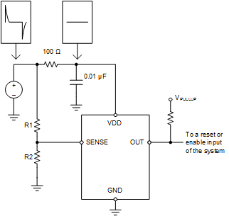
GUID-9FA64400-F242-4058-8B8E-3B155C270B9F-low.gif Figure 7-5 Using an RC Filter to Remove High-Frequency Disturbances on VDD