SGLS228C December 2003 – September 2015 TPS3805H33-Q1
PRODUCTION DATA.
- 1 Features
- 2 Applications
- 3 Description
- 4 Revision History
- 5 Device Comparison Table
- 6 Pin Configuration and Functions
- 7 Specifications
- 8 Detailed Description
- 9 Application and Implementation
- 10Power Supply Recommendations
- 11Layout
- 12Device and Documentation Support
- 13Mechanical, Packaging, and Orderable Information
Package Options
Refer to the PDF data sheet for device specific package drawings
Mechanical Data (Package|Pins)
- DCK|5
Thermal pad, mechanical data (Package|Pins)
Orderable Information
7 Specifications
7.1 Absolute Maximum Ratings
over operating free-air temperature range (unless otherwise noted)(1)| MIN | MAX | UNIT | |||
|---|---|---|---|---|---|
| VDD | Supply voltage(2) | 7 | 7 | V | |
| Voltage applied to all other pins(2) | –0.3 | 7 | V | ||
| IOL | Maximum low-level output current | 5 | mA | ||
| IOH | Maximum high-level output current | –5 | mA | ||
| IIK | Input clamp current | VI < 0 or VI > VDD | ±10 | mA | |
| IOK | Output clamp current | VO < 0 or VO > VDD | ±10 | mA | |
| PD | Continuous total power dissipation | See Dissipation Ratings | |||
| TA | Operating free-air temperature | –40 | 125 | °C | |
| Tsolder | Soldering temperature | 260 | °C | ||
| Tstg | Storage temperature | –65 | 150 | °C | |
(1) Stresses beyond those listed under Absolute Maximum Ratings may cause permanent damage to the device. These are stress ratings only, and functional operation of the device at these or any other conditions beyond those indicated under Recommended Operating Conditions is not implied. Exposure to absolute-maximum-rated conditions for extended periods may affect device reliability.
(2) All voltage values are with respect to GND. For reliable operation, the device should not be continuously operated at 7 V for more than t = 1000 h.
7.2 ESD Ratings
| VALUE | UNIT | |||
|---|---|---|---|---|
| V(ESD) | Electrostatic discharge | Human body model (HBM), per AEC Q100-002(1) | ±2000 | V |
| Charged-device model (CDM), per AEC Q100-011 | ±1000 | |||
(1) AEC Q100-002 indicates that HBM stressing shall be in accordance with the ANSI/ESDA/JEDEC JS-001 specification.
7.3 Recommended Operating Conditions
| MIN | MAX | UNIT | ||
|---|---|---|---|---|
| VDD | Supply voltage | 1.3 | 6 | V |
| VI | Input voltage | 0 | VDD + 0.3 | V |
| TA | Operating free-air temperature | –40 | 125 | °C |
7.4 Thermal Information
| THERMAL METRIC(1) | TPS3803x-Q1 TPS3805x-Q1 | UNIT | |
|---|---|---|---|
| DCK (SC-70) | |||
| 5 PINS | |||
| RθJA | Junction-to-ambient thermal resistance | 246.6 | °C/W |
| RθJC(top) | Junction-to-case (top) thermal resistance | 68.2 | °C/W |
| RθJB | Junction-to-board thermal resistance | 78.4 | °C/W |
| ψJT | Junction-to-top characterization parameter | 0.9 | °C/W |
| ψJB | Junction-to-board characterization parameter | 77.7 | °C/W |
| RθJC(bot) | Junction-to-case (bottom) thermal resistance | N/A | °C/W |
(1) For more information about traditional and new thermal metrics, see the Semiconductor and IC Package Thermal Metrics application report, SPRA953.
7.5 Electrical Characteristics
over operating free-air temperature range (unless otherwise noted)| PARAMETER | TEST CONDITIONS | MIN | TYP | MAX | UNIT | ||
|---|---|---|---|---|---|---|---|
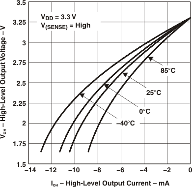
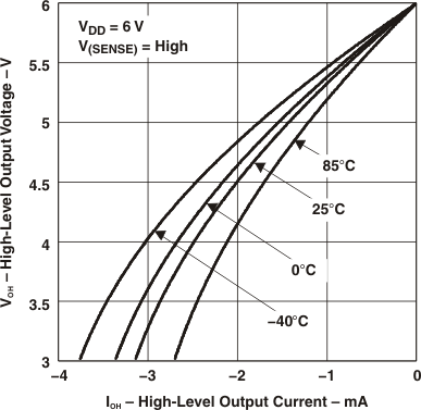
| VOH | High-level output voltage (TPS3805 only) | VDD = 1.5 V, IOH = –0.5 mA | 0.8 × VDD | V | |||
| VDD = 3.3 V, IOH = –1 mA | |||||||
| VDD = 6 V, IOH = –1.5 mA | |||||||
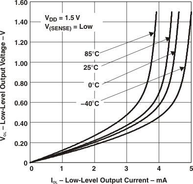
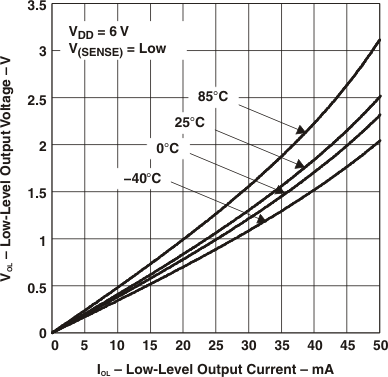
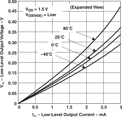
| VOL | Low-level output voltage | VDD = 1.5 V, IOL = 1 mA | 0.3 | V | |||
| VDD = 3.3 V, IOL = 2 mA | |||||||
| VDD = 6 V, IOL = 3 mA | |||||||
| Power-up reset voltage(1) | VIT > 1.5 V, TA = 25°C | 0.8 | V | ||||
| VIT ≤ 1.5 V, TA = 25°C | 1 | ||||||
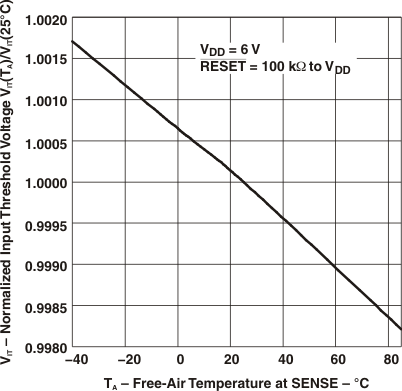
| VIT | Negative-going input threshold voltage(2) | SENSE | 1.2 | 1.226 | 1.244 | V | |
| TPS3803G15 | 1.379 | 1.4 | 1.421 | ||||
| TPS3805H33 | 3.004 | 3.05 | 3.096 | ||||
| Vhys | Hysteresis | 1.2 V < VIT < 2.5 V | 15 | mV | |||
| 2.5 V < VIT < 3.5 V | 30 | ||||||
| II | Input current | SENSE | –25 | 25 | nA | ||
| IOH | High-level output current at RESET | Open drain only | VDD = VIT + 0.2 V, VOH = VDD | 300 | nA | ||
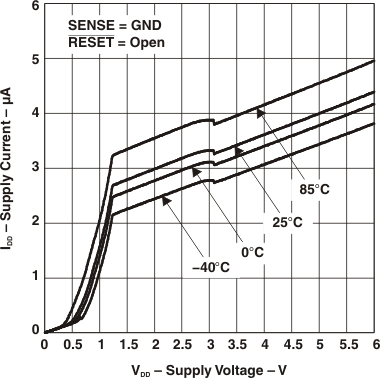
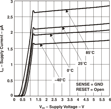
| IDD | Supply current | TPS3803-01 | VDD = 3.3 V, Output unconnected | 2 | 4 | μA | |
| TPS3805, TPS3803G15 | 3 | 5 | |||||
| TPS3803-01 | VDD = 6 V, Output unconnected | 2 | 4 | ||||
| TPS3805, TPS3803G15 | 4 | 6 | |||||
| CI | Input capacitance | VI = 0 V to VDD | 1 | pF | |||
(1) The lowest supply voltage at which RESET (VOL(max) = 0.2 V, IOL = 50 μA) becomes active. tr(VDD) ≥ 15 μs/V.
(2) To ensure the best stability of the threshold voltage, place a bypass capacitor (ceramic, 0.1-μF) near the supply terminals.
7.6 Timing Requirements
RL = 1 MΩ, CL = 50 pF, TA = –40°C to 125°C (unless otherwise noted)| MIN | MAX | UNIT | ||||
|---|---|---|---|---|---|---|
| tw | Pulse duration | VDD | VIH = 1.05 × VIT, VIL = 0.95 × VIT | 5.5 | μs | |
| SENSE | ||||||
7.7 Switching Characteristics
RL = 1 MΩ, CL = 50 pF, TA = –40°C to 125°C (unless otherwise noted)| PARAMETER | TEST CONDITIONS | MIN | TYP | MAX | UNIT | ||
|---|---|---|---|---|---|---|---|
| tPHL | Propagation (delay) time, high-to-low-level output | VDD to RESET delay | VIH = 1.05 × VIT, VIL = 0.95 × VIT | 5 | 100 | μs | |
| SENSE to RESET delay | |||||||
| tPLH | Propagation (delay) time, low-to-high-level output | VDD to RESET delay | VIH = 1.05 × VIT, VIL = 0.95 × VIT | 5 | 100 | μs | |
| SENSE to RESET delay μA | |||||||
7.8 Dissipation Ratings
| PACKAGE | POWER RATING TA < 25°C |
DERATING FACTOR ABOVE TA = 25°C |
POWER RATING TA = 70°C |
POWER RATING TA = 85°C |
|---|---|---|---|---|
| DCK | 321 mW | 2.6 mW/°C | 206 mW | 167 mW |
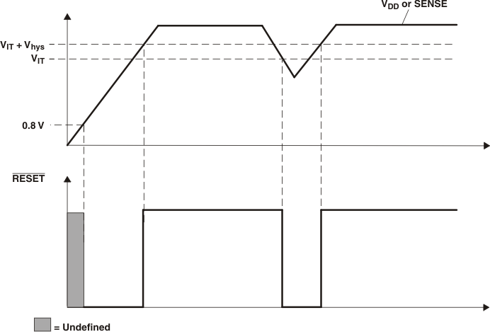 Figure 1. Timing Requirements
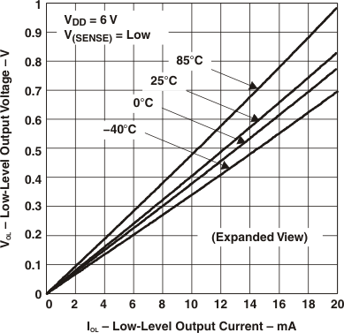
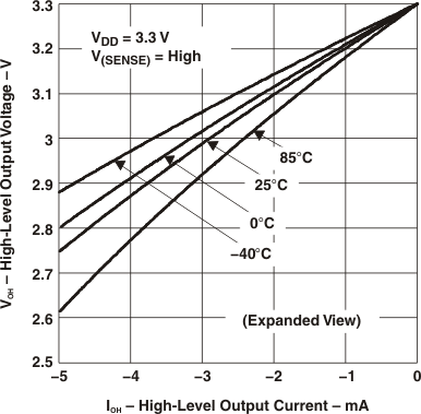
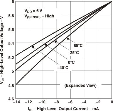
7.9 Typical Characteristics
