SBVS103D April 2008 – December 2014 TPS3808-EP
PRODUCTION DATA.
- 1 Features
- 2 Applications
- 3 Description
- 4 Revision History
- 5 Pin Configuration and Functions
- 6 Specifications
- 7 Detailed Description
- 8 Application and Implementation
- 9 Power Supply Recommendations
- 10Layout
- 11Device and Documentation Support
- 12Mechanical, Packaging, and Orderable Information
Package Options
Mechanical Data (Package|Pins)
- DBV|6
Thermal pad, mechanical data (Package|Pins)
Orderable Information
7 Detailed Description
7.1 Overview
The TPS3808 microprocessor supervisory product family is designed to assert a RESET signal when either the SENSE pin voltage drops below VIT or the manual reset (MR) is driven low. The RESET output remains asserted for a user-adjustable time after both the manual reset (MR) and SENSE voltages return above the respective thresholds.
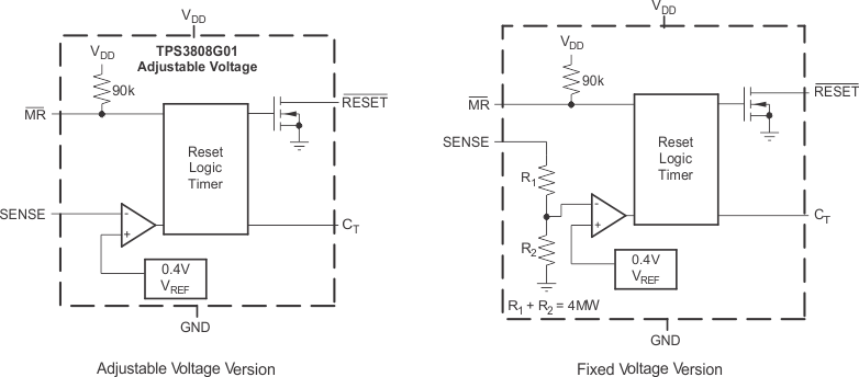
7.2 Functional Block Diagrams
7.3 Feature Description
A broad range of voltage threshold and reset delay time adjustments are available for the TPS3808 device, allowing these devices to be used in a wide array of applications. Reset threshold voltages can be factory-set from 0.82 V to 3.3 V or from 4.4 V to 5.0 V, while the TPS3808G01 can be set to any voltage above 0.405 V using an external resistor divider. Two preset delay times are also user-selectable: connecting the CT pin to VDD results in a 300 ms reset delay, while leaving the CT pin open yields a 20-ms reset delay. In addition, connecting a capacitor between CT and GND allows the designer to select any reset delay period from 1.25 ms to 10 s.
7.4 Device Functional Modes
The TPS3808 has two functional modes:
- MR high: in this mode, RESET is high or low depending on the value of the SENSE pin relative to VIT.
- MR low: in this mode, RESET is held low regarldess of the value of the SENSE pin.