SBVS103D April 2008 – December 2014 TPS3808-EP
PRODUCTION DATA.
- 1 Features
- 2 Applications
- 3 Description
- 4 Revision History
- 5 Pin Configuration and Functions
- 6 Specifications
- 7 Detailed Description
- 8 Application and Implementation
- 9 Power Supply Recommendations
- 10Layout
- 11Device and Documentation Support
- 12Mechanical, Packaging, and Orderable Information
Package Options
Mechanical Data (Package|Pins)
- DBV|6
Thermal pad, mechanical data (Package|Pins)
Orderable Information
5 Pin Configuration and Functions
DBV PACKAGE
SOT-23
(TOP VIEW)
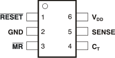
Pin Functions
| PIN | I/O | DESCRIPTION | |
|---|---|---|---|
| NAME | NO. | ||
| RESET | 1 | O | RESET is an open-drain output that is driven to a low impedance state when RESET is asserted (either the SENSE input is lower than the threshold voltage (VIT) or the MR pin is set to a logic low). RESET remains low (asserted) for the reset period after both SENSE is above VIT and MR is set to a logic high. A pullup resistor from 10 kΩ to 1 MΩ should be used on this pin, and allows the reset pin to attain voltages higher than VDD. |
| GND | 2 | — | Ground |
| MR | 3 | I | Driving the manual reset pin (MR) low asserts RESET. MR is internally tied to VDD by a 90kΩ pullup resistor. |
| CT | 4 | I | Reset period programming pin. Connecting this pin to VDD through a 40-kΩ to 200-kΩ resistor or leaving it open results in fixed delay times (see Switching Characteristics). Connecting this pin to a ground referenced capacitor ≥ 100 pF gives a user-programmable delay time. See the Selecting the Reset Delay Time section for more information. |
| SENSE | 5 | I | This pin is connected to the voltage to be monitored. If the voltage at this terminal drops below the threshold voltage VIT, then RESET is asserted. |
| VDD | 6 | I | Supply voltage. It is good analog design practice to place a 0.1-μF ceramic capacitor close to this pin. |