SBVS103D April 2008 – December 2014 TPS3808-EP
PRODUCTION DATA.
- 1 Features
- 2 Applications
- 3 Description
- 4 Revision History
- 5 Pin Configuration and Functions
- 6 Specifications
- 7 Detailed Description
- 8 Application and Implementation
- 9 Power Supply Recommendations
- 10Layout
- 11Device and Documentation Support
- 12Mechanical, Packaging, and Orderable Information
Package Options
Mechanical Data (Package|Pins)
- DBV|6
Thermal pad, mechanical data (Package|Pins)
Orderable Information
6 Specifications
6.1 Absolute Maximum Ratings
Over operating junction temperature range, unless otherwise noted.(1)| MIN | MAX | UNIT | |
|---|---|---|---|
| Input voltage, VDD | –0.3 | 7.0 | V |
| CT voltage, VCT | –0.3 | VDD + 0.3 | |
| Other voltage: VRESET, VMR, VSENSE | –0.3 | 7 | |
| RESET pin current | 5 | mA | |
| Operating junction temperature, TJ(2) | –55 | 150 | °C |
| Storage temperature, Tstg | –65 | 150 |
(1) Stresses beyond those listed under Absolute Maximum Ratings may cause permanent damage to the device. These are stress ratings only, which do not imply functional operation of the device at these or any other conditions beyond those indicated under Recommended Operating Conditions. Exposure to absolute-maximum-rated conditions for extended periods may affect device reliability.
(2) As a result of the low dissipated power in this device, it is assumed that TJ = TA.
6.2 ESD Ratings
| VALUE | UNIT | ||||
|---|---|---|---|---|---|
| V(ESD) | Electrostatic discharge | Human body model (HBM), per ANSI/ESDA/JEDEC JS-001, all pins(1) | ±3000 | V | |
| Charged device model (CDM), per JEDEC specification JESD22-C101, all pins(2) | ±1000 | ||||
(1) JEDEC document JEP155 states that 500-V HBM allows safe manufacturing with a standard ESD control process.
(2) JEDEC document JEP157 states that 250-V CDM allows safe manufacturing with a standard ESD control process.
6.3 Recommended Operating Conditions
over operating free-air temperature range (unless otherwise noted)| MIN | NOM | MAX | UNIT | ||
|---|---|---|---|---|---|
| VDD | Input supply range | 1.7 | 6.5 | V | |
| Power-up reset voltage | VOL (max) = 0.2 V, IRESET = 15 μA | 0.8 | V | ||
6.4 Thermal Information
| THERMAL METRIC(1) | TPS3808-EP | UNIT | |
|---|---|---|---|
| DBV | |||
| 6 PINS | |||
| RθJA | Junction-to-ambient thermal resistance | 180.9 | °C/W |
| RθJC(top) | Junction-to-case (top) thermal resistance | 117.8 | |
| RθJB | Junction-to-board thermal resistance | 27.8 | |
| ψJT | Junction-to-top characterization parameter | 1.12 | |
| ψJB | Junction-to-board characterization parameter | 27.3 | |
(1) For more information about traditional and new thermal metrics, see the IC Package Thermal Metrics application report, SPRA953.
6.5 Electrical Characteristics
1.7 V ≤ VDD ≤ 6.5 V, RLRESET = 100 kΩ, CLRESET = 50 pF, over operating temperature range (TJ = –55°C to +125°C), unless otherwise noted. Typical values are at TJ = +25°C.| PARAMETER | TEST CONDITIONS | MIN | TYP | MAX | UNIT | |||
|---|---|---|---|---|---|---|---|---|
| VDD | Input supply range | 1.7 | 6.5 | V | ||||
| IDD | Supply current (current into VDD pin) | VDD = 3.3 V, RESET not asserted MR, RESET, CT open |
2.4 | 5.0 | μA | |||
| VDD = 6.5 V, RESET not asserted MR, RESET, CT open |
2.7 | 6.0 | ||||||
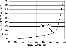
| VOL | Low-level output voltage | 1.3 V ≤ VDD < 1.8 V, IOL = 0.4 mA | 0.3 | V | ||||
| 1.8 V ≤ VDD ≤ 6.5 V, IOL = 1.0 mA | 0.4 | |||||||
| Power-up reset voltage(1) | VOL (max) = 0.2 V, IRESET = 15 μA | 0.8 | ||||||
| VIT | Negative-going input threshold accuracy | TPS3808G01 | –2.0% | ±1.0% | +2.0% | |||
| VIT ≤ 3.3 V | –1.7% | ±0.5% | +1.7% | |||||
| 3.3 V < VIT ≤ 5.0 V | –2.0% | ±1.0% | +2.0% | |||||
| VHYS | Hysteresis on VIT pin | TPS3808G01 | 1.5% | 3.0% | VIT | |||
| Fixed versions | 1.0% | 2.5% | ||||||
| RMR | MR Internal pullup resistance | 70 | 90 | kΩ | ||||
| ISENSE | Input current at SENSE pin | TPS3808G01 | VSENSE = VIT | –25 | 25 | nA | ||
| Fixed versions | VSENSE = 6.5 V | 1.7 | μA | |||||
| IOH | RESET leakage current | VRESET = 6.5 V, RESET not asserted | 300 | nA | ||||
| CIN | Input capacitance, any pin | CT pin | VIN = 0 V to VDD | 5 | pF | |||
| Other pins | VIN = 0 V to 6.5 V | 5 | ||||||
| VIL | MR logic low input | 0 | 0.3 VDD | V | ||||
| VIH | MR logic high input | 0.7 VDD | VDD | |||||
| θJA | Thermal resistance, junction-to-ambient | 290 | °C/W | |||||
(1) The lowest supply voltage (VDD) at which RESET becomes active. Trise(VDD) ≥ 15 μs/V.
6.6 Switching Characteristics
1.7 V ≤ VDD ≤ 6.5 V, RLRESET = 100 kΩ, CLRESET = 50 pF, over operating temperature range (TJ = –55°C to +125°C), unless otherwise noted. Typical values are at TJ = +25°C.| PARAMETER | TEST CONDITIONS | MIN | TYP | MAX | UNIT | ||
|---|---|---|---|---|---|---|---|
| tw | Input pulse width to RESET | SENSE | VIH = 1.05 VIT, VIL = 0.95 VIT | 20 | μs | ||
| MR | VIH = 0.7 VDD, VIL = 0.3 VDD | 0.001 | |||||
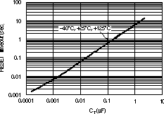
| td | RESET delay time | CT = Open | See Timing Diagram | 12 | 20 | 29 | ms |
| CT = VDD | 180 | 300 | 440 | ||||
| CT = 100 pF | 0.75 | 1.25 | 1.8 | ||||
| CT = 180 nF | 0.7 | 1.2 | 1.8 | s | |||
| tpHL | Propagation delay | MR to RESET | VIH = 0.7 VDD, VIL = 0.3 VDD | 150 | ns | ||
| High-to-low level RESET delay | SENSE to RESET | VIH = 1.05 VIT, VIL = 0.95 VIT | 20 | μs | |||
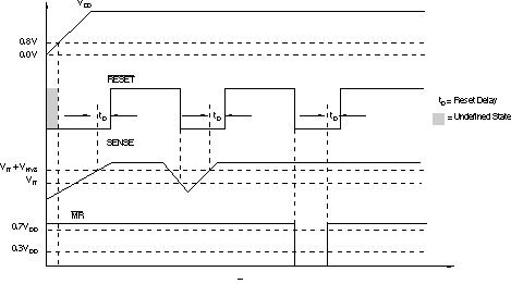 Figure 1. TPS3808 Timing Diagram Showing MR and SENSE Reset Timing
Table 1. Truth Table
| MR | SENSE > VIT | RESET |
|---|---|---|
| L | 0 | L |
| L | 1 | L |
| H | 0 | L |
| H | 1 | H |
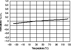
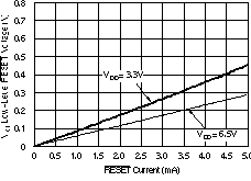
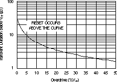
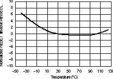
6.7 Typical Characteristics
At TJ = +25°C, VDD = 3.3 V, RLRESET = 100kΩ, and CLRESET = 50pF, unless otherwise noted.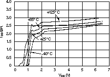
| CT = Open, CT = VDD, CT = Any |