SBVS050M May 2004 – March 2023 TPS3808
PRODUCTION DATA
- 1 Features
- 2 Applications
- 3 Description
- 4 Revision History
- 5 Device Voltage Thresholds
- 6 Pin Configuration and Functions
- 7 Specifications
- 8 Detailed Description
- 9 Application and Implementation
- 10Power Supply Recommendations
- 11Layout
- 12Device and Documentation Support
- 13Mechanical, Packaging, and Orderable Information
Package Options
Mechanical Data (Package|Pins)
Thermal pad, mechanical data (Package|Pins)
- DRV|6
Orderable Information
3 Description
The TPS3808 family of microprocessor supervisory circuits monitors system voltages from 0.4 V to 5 V, asserting an open-drain RESET signal when the SENSE voltage drops below a preset threshold or when the manual reset ( MR) pin drops to a logic low. The RESET output remains low for the user-adjustable delay time after the SENSE voltage and manual reset ( MR) return above the respective thresholds.
The TPS3808 device uses a precision reference to achieve 0.5% threshold accuracy for VIT ≤ 3.3 V. The reset delay time can be set to 20 ms by disconnecting the CT pin, 300 ms by connecting the CT pin to VDD using a resistor, or can be user-adjusted between 1.25 ms and 10 s by connecting the CT pin to an external capacitor. The TPS3808 device has a very low typical quiescent current of 2.4 μA, so it is well-suited to battery-powered applications. It is available in the SOT-23 and 2-mm × 2-mm WSON packages, and is fully specified over a temperature range of –40°C to 125°C (TJ).
| PART NUMBER | PACKAGE(1) | BODY SIZE (NOM) |
|---|---|---|
| TPS3808 | SOT-23 (6) | 2.90 mm x 1.60 mm |
| WSON (6) | 2.00 mm x 2.00 mm |
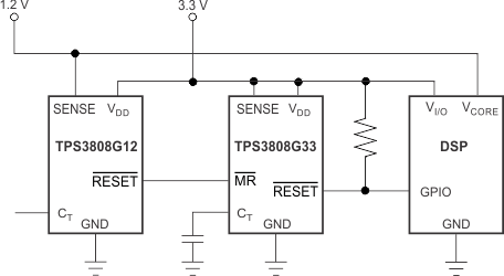
 Typical Application
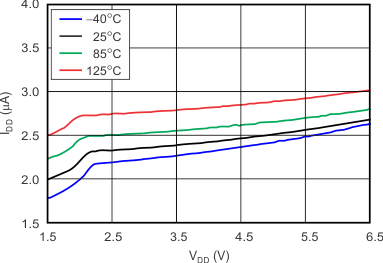
 Supply Current vs Supply
Voltage