SLVS753C February 2007 – November 2016 TPS40180
PRODUCTION DATA.
- 1 Features
- 2 Applications
- 3 Description
- 4 Revision History
- 5 Pin Configuration and Functions
- 6 Specifications
-
7 Detailed Description
- 7.1 Overview
- 7.2 Functional Block Diagram
- 7.3
Feature Description
- 7.3.1 Current Sensing and Overcurrent Detection
- 7.3.2 Hiccup Fault Recovery
- 7.3.3 Selecting Current Sense Network Components
- 7.3.4 PGOOD Functionality
- 7.3.5 Output Overvoltage and Undervoltage Protection
- 7.3.6 Overtemperature Protection
- 7.3.7 eTRIM™
- 7.3.8 Connections Between Controllers for Stacking
- 7.3.9 VSH Line in the Multiphase
- 7.4 Device Functional Modes
- 7.5 Programming
-
8 Application and Implementation
- 8.1 Application Information
- 8.2
Typical Applications
- 8.2.1
Single Output Synchronous Buck Converter
- 8.2.1.1 Design Requirements
- 8.2.1.2
Detailed Design Procedure
- 8.2.1.2.1 Inductor Selection
- 8.2.1.2.2 Output Capacitor Selection
- 8.2.1.2.3 Input Capacitor Selection
- 8.2.1.2.4 MOSFET Selection
- 8.2.1.2.5
Peripheral Component Design
- 8.2.1.2.5.1 Switching Frequency Setting (RT)
- 8.2.1.2.5.2 Output Voltage Setting (FB)
- 8.2.1.2.5.3 Current Sensing Network Design (CS+, CS-)
- 8.2.1.2.5.4 Overcurrent Protection (ILIM)
- 8.2.1.2.5.5 VREG (PVCC)
- 8.2.1.2.5.6 BP5
- 8.2.1.2.5.7 Phase Select (PSEL)
- 8.2.1.2.5.8 VSHARE (VSH)
- 8.2.1.2.5.9 Powergood (PGOOD)
- 8.2.1.2.5.10 Undervoltage Lockout (UVLO)
- 8.2.1.2.5.11 Clock Synchronization (CLKIO)
- 8.2.1.2.5.12 Bootstrap Capacitor
- 8.2.1.2.5.13 Soft Start (SS)
- 8.2.1.2.5.14 Remote Sense
- 8.2.1.2.5.15 Feedback Compensator Design
- 8.2.1.3 Application Curves
- 8.2.2 Simultaneous Tracking With TPS40180 Devices
- 8.2.3 2-Phase Single Output With TPS40180
- 8.2.1
Single Output Synchronous Buck Converter
- 9 Power Supply Recommendations
- 10Layout
- 11Device and Documentation Support
- 12Mechanical, Packaging, and Orderable Information
Package Options
Mechanical Data (Package|Pins)
- RGE|24
Thermal pad, mechanical data (Package|Pins)
- RGE|24
Orderable Information
1 Features
- Stackable to 8 Phases, Multiple Controllers Can Occupy Any Phase
- 2-V to 40-V Power Stage Operation Range
- eTrim™ in System Reference Voltage Trim to Tighten Overall Output Voltage Tolerance, Reference is Better Than 0.75% Untrimmed
- VDD From 4.5 V to 15 V, With Internal 5-V Regulator
- Supports Output Voltage From 0.7 V to 5.8 V
- Supports Prebiased Outputs
- 10-µA Shutdown Current
- Programmable Switching Frequency up to 1-MHz per Phase
- Current Feedback Control With Forced Current Sharing (Patents Pending)
- Resistive Divider Sets Input Undervoltage Lockout and Hysteresis
- True Remote Sensing Differential Amplifier
- Resistive or Inductor’s DCR Current Sensing
2 Applications
- Graphic Cards
- Servers
- Networking Equipment
- Telecommunications Equipment
- Distributed DC Power Systems
3 Description
The TPS40180 is a stackable single-phase synchronous buck controller. Stacking allows a modular power supply design where multiple modules can be connected in parallel to achieve higher power capability. Stacked modules can be configured at the same switching frequency with interleaved phase shift to reduce input and output ripple current. Stacked modules can also be configured to generate separate output rails at the same time as different phase shift to reduce input ripple current.
The TPS40180 is optimized for low-output voltage (from 0.7-V to 5.8-V), high-output current applications powered from a 2-V to 40-V supply.
With eTrim™, the TPS40180 gives the user the capability to trim the reference voltage on the device to compensate for external component tolerances, tightening the overall system accuracy and allowing tighter specifications for output voltage of the converter.
Device Information(1)
| PART NUMBER | PACKAGE | BODY SIZE (NOM) |
|---|---|---|
| TPS40180 | VQFN (24) | 4.00 mm × 4.00 mm |
- For all available packages, see the orderable addendum at the end of the data sheet.
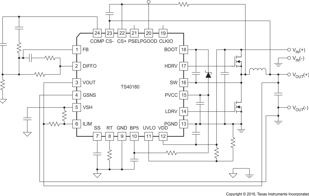
Typical Application
