SLUS739F September 2006 – January 2016 TPS40200-Q1
PRODUCTION DATA.
- 1 Features
- 2 Applications
- 3 Description
- 4 Revision History
- 5 Pin Configuration and Functions
- 6 Specifications
- 7 Detailed Description
-
8 Application and Implementation
- 8.1 Application Information
- 8.2
Typical Applications
- 8.2.1
Buck Regulator, 8-V to 12-V Input, 3.3-V or 5-V Output at 2.5 A
- 8.2.1.1 Design Requirements
- 8.2.1.2 Detailed Design Procedure
- 8.2.1.3 Application Curves
- 8.2.2 Application 2: 18-V to 50-V Input, 16-V Output at 1 A
- 8.2.3 Application 3: Wide-Input-Voltage LED Constant-Current Driver
- 8.2.1
Buck Regulator, 8-V to 12-V Input, 3.3-V or 5-V Output at 2.5 A
- 9 Power Supply Recommendations
- 10Layout
- 11Device and Documentation Support
- 12Mechanical, Packaging, and Orderable Information
Package Options
Mechanical Data (Package|Pins)
- D|8
Thermal pad, mechanical data (Package|Pins)
Orderable Information
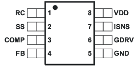
5 Pin Configuration and Functions
D Package
8-Pin SOIC
Top View

Pin Functions
| PIN | I/O | DESCRIPTION | |
|---|---|---|---|
| NO. | NAME | ||
| 1 | RC | I | Switching frequency setting RC network. Connect a capacitor from RC pin to GND pin and a resistor from VIN pin to RC pin. The device may be synchronized to an external clock by connecting an open-drain output to this pin and pulling it to GND. The pulse width for synchronization should not be excessive (see Detailed Description). |
| 2 | SS | I | Soft-start programming. Connect capacitor from SS to GND to program soft-start time. Pulling this pin below 150 mV causes the output switching to stop, placing the device in a shutdown state. The pin also functions as a restart timer for overcurrent events. |
| 3 | COMP | O | Error amplifier output. Connect control loop compensation network from COMP to FB. |
| 4 | FB | I | Error amplifier inverting input. Connect feedback resistor network center tap to this pin. |
| 5 | GND | — | Device ground |
| 6 | GDRV | O | Driver output for external P-channel MOSFET |
| 7 | ISNS | I | Current-sense comparator input. Connect a current sense resistor between ISNS and VDD in order to set desired overcurrent threshold. |
| 8 | VDD | I | System input voltage. Connect local bypass capacitor from VDD to GND. |