SLUS964D NOVEMBER 2009 – March 2018 TPS40303 , TPS40304 , TPS40305
PRODUCTION DATA.
- 1 Features
- 2 Applications
- 3 Description
- 4 Revision History
- 5 Pin Configuration and Functions
- 6 Specifications
- 7 Detailed Description
-
8 Application and Implementation
- 8.1 Application Information
- 8.2
Typical Applications
- 8.2.1
Using the TPS40305 for a 12-V to 1.8-V Point-of-Load Synchronous Buck Regulator
- 8.2.1.1 Design Requirements
- 8.2.1.2
Detailed Design Procedure
- 8.2.1.2.1 Custom Design With WEBENCH® Tools
- 8.2.1.2.2 Selecting the Switching Frequency
- 8.2.1.2.3 Inductor Selection (L1)
- 8.2.1.2.4 Output Capacitor Selection (C12)
- 8.2.1.2.5 Peak Current Rating of Inductor
- 8.2.1.2.6 Input Capacitor Selection (C8)
- 8.2.1.2.7 MOSFET Switch Selection (Q1 and Q2)
- 8.2.1.2.8 Bootstrap Capacitor (C6)
- 8.2.1.2.9 VDD Bypass Capacitor (C7)
- 8.2.1.2.10 BP Bypass Capacitor (C5)
- 8.2.1.2.11 Short-Circuit Protection (R11)
- 8.2.1.2.12 Feedback Divider (R4, R5)
- 8.2.1.2.13 Compensation: (C2, C3, C4, R3, R6)
- 8.2.1.3 Application Curves
- 8.2.2
A High-Current, Low-Voltage Design Using the TPS40304
- 8.2.2.1 Design Requirements
- 8.2.2.2
Detailed Design Procedure
- 8.2.2.2.1 Selecting the Switching Frequency
- 8.2.2.2.2 Inductor Selection (L1)
- 8.2.2.2.3 Output Capacitor Selection (C12)
- 8.2.2.2.4 Peak Current Rating of Inductor
- 8.2.2.2.5 Input Capacitor Selection (C8)
- 8.2.2.2.6 MOSFET Switch Selection (Q1 and Q2)
- 8.2.2.2.7 Bootstrap Capacitor (C6)
- 8.2.2.2.8 VDD Bypass Capacitor (C7)
- 8.2.2.2.9 BP Bypass Capacitor (C5)
- 8.2.2.2.10 Short-Circuit Protection (R11)
- 8.2.2.2.11 Feedback Divider (R4, R5)
- 8.2.2.2.12 Compensation: (C2, C3, C4, R3, R6)
- 8.2.2.3 Application Curves
- 8.2.3
A Synchronous Buck Application Using the TPS40303
- 8.2.3.1 Design Requirements
- 8.2.3.2
Detailed Design Procedure
- 8.2.3.2.1 Selecting the Switching Frequency
- 8.2.3.2.2 Inductor Selection (L1)
- 8.2.3.2.3 Output Capacitor Selection (C12)
- 8.2.3.2.4 Peak Current Rating of Inductor
- 8.2.3.2.5 Input Capacitor Selection (C8)
- 8.2.3.2.6 MOSFET Switch Selection (Q1 and Q2)
- 8.2.3.2.7 Bootstrap Capacitor (C6)
- 8.2.3.2.8 VDD Bypass Capacitor (C7)
- 8.2.3.2.9 BP Bypass Capacitor (C5)
- 8.2.3.2.10 Short-Circuit Protection (R11)
- 8.2.3.2.11 Feedback Divider (R4, R5)
- 8.2.3.2.12 Compensation: (C2, C3, C4, R3, R6)
- 8.2.3.3 Application Curves
- 8.2.1
Using the TPS40305 for a 12-V to 1.8-V Point-of-Load Synchronous Buck Regulator
- 9 Power Supply Recommendations
- 10Layout
- 11Device and Documentation Support
- 12Mechanical, Packaging, and Orderable Information
Package Options
Mechanical Data (Package|Pins)
- DRC|10
Thermal pad, mechanical data (Package|Pins)
- DRC|10
Orderable Information
7.3.2 Enable Functionality, Start-Up Sequence and Timing
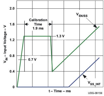
After input power is applied, an internal current source of 40 µA starts to charge up the soft-start capacitor connected from EN/SS to GND. When the voltage across that capacitor increases to 0.7 V, it enables the internal BP regulator followed by a calibration. The total calibration time is about 1.9 ms. See Figure 13. During the calibration, the device performs in the following way. It disables the LDRV drive and injects an internal 10-µA current source to the resistor connected from LDRV to GND. The voltage developed across that resistor is then sampled and latched internally as the OCP trip level until one cycles the input or toggles the EN/SS.
 Figure 13. Start-Up Sequence and Timing
The voltage at EN/SS is internally clamped to 1.3 V before and/or during calibration to minimize the discharging time once calibration. The discharging current is from an internal current source of 140 µA and it pulls the voltage down to 0.4 V. The discharging current then initiates the soft-start by charging up the capacitor using an internal current source of 10 µA. The resulting voltage ramp on this pin is used as a second noninverting input to the error amplifier after an 800 mV (typical) downward level-shift; therefore, actual soft-start does not occur until the voltage at this pin reaches 800 mV.
If EN/SS is left floating, the controller starts automatically. EN/SS must be pulled down to less than 270 mV to ensure that the chip is in shutdown mode.