SLUS964D NOVEMBER 2009 – March 2018 TPS40303 , TPS40304 , TPS40305
PRODUCTION DATA.
- 1 Features
- 2 Applications
- 3 Description
- 4 Revision History
- 5 Pin Configuration and Functions
- 6 Specifications
- 7 Detailed Description
-
8 Application and Implementation
- 8.1 Application Information
- 8.2
Typical Applications
- 8.2.1
Using the TPS40305 for a 12-V to 1.8-V Point-of-Load Synchronous Buck Regulator
- 8.2.1.1 Design Requirements
- 8.2.1.2
Detailed Design Procedure
- 8.2.1.2.1 Custom Design With WEBENCH® Tools
- 8.2.1.2.2 Selecting the Switching Frequency
- 8.2.1.2.3 Inductor Selection (L1)
- 8.2.1.2.4 Output Capacitor Selection (C12)
- 8.2.1.2.5 Peak Current Rating of Inductor
- 8.2.1.2.6 Input Capacitor Selection (C8)
- 8.2.1.2.7 MOSFET Switch Selection (Q1 and Q2)
- 8.2.1.2.8 Bootstrap Capacitor (C6)
- 8.2.1.2.9 VDD Bypass Capacitor (C7)
- 8.2.1.2.10 BP Bypass Capacitor (C5)
- 8.2.1.2.11 Short-Circuit Protection (R11)
- 8.2.1.2.12 Feedback Divider (R4, R5)
- 8.2.1.2.13 Compensation: (C2, C3, C4, R3, R6)
- 8.2.1.3 Application Curves
- 8.2.2
A High-Current, Low-Voltage Design Using the TPS40304
- 8.2.2.1 Design Requirements
- 8.2.2.2
Detailed Design Procedure
- 8.2.2.2.1 Selecting the Switching Frequency
- 8.2.2.2.2 Inductor Selection (L1)
- 8.2.2.2.3 Output Capacitor Selection (C12)
- 8.2.2.2.4 Peak Current Rating of Inductor
- 8.2.2.2.5 Input Capacitor Selection (C8)
- 8.2.2.2.6 MOSFET Switch Selection (Q1 and Q2)
- 8.2.2.2.7 Bootstrap Capacitor (C6)
- 8.2.2.2.8 VDD Bypass Capacitor (C7)
- 8.2.2.2.9 BP Bypass Capacitor (C5)
- 8.2.2.2.10 Short-Circuit Protection (R11)
- 8.2.2.2.11 Feedback Divider (R4, R5)
- 8.2.2.2.12 Compensation: (C2, C3, C4, R3, R6)
- 8.2.2.3 Application Curves
- 8.2.3
A Synchronous Buck Application Using the TPS40303
- 8.2.3.1 Design Requirements
- 8.2.3.2
Detailed Design Procedure
- 8.2.3.2.1 Selecting the Switching Frequency
- 8.2.3.2.2 Inductor Selection (L1)
- 8.2.3.2.3 Output Capacitor Selection (C12)
- 8.2.3.2.4 Peak Current Rating of Inductor
- 8.2.3.2.5 Input Capacitor Selection (C8)
- 8.2.3.2.6 MOSFET Switch Selection (Q1 and Q2)
- 8.2.3.2.7 Bootstrap Capacitor (C6)
- 8.2.3.2.8 VDD Bypass Capacitor (C7)
- 8.2.3.2.9 BP Bypass Capacitor (C5)
- 8.2.3.2.10 Short-Circuit Protection (R11)
- 8.2.3.2.11 Feedback Divider (R4, R5)
- 8.2.3.2.12 Compensation: (C2, C3, C4, R3, R6)
- 8.2.3.3 Application Curves
- 8.2.1
Using the TPS40305 for a 12-V to 1.8-V Point-of-Load Synchronous Buck Regulator
- 9 Power Supply Recommendations
- 10Layout
- 11Device and Documentation Support
- 12Mechanical, Packaging, and Orderable Information
Package Options
Mechanical Data (Package|Pins)
- DRC|10
Thermal pad, mechanical data (Package|Pins)
- DRC|10
Orderable Information
6.6 Typical Characteristics
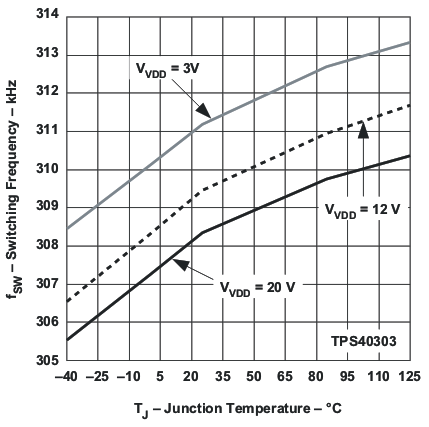 Figure 1. Switching Frequency vs Junction Temperature
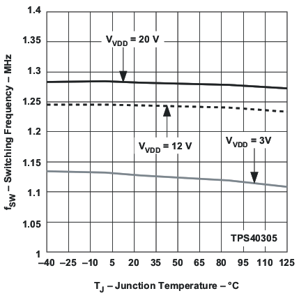 Figure 3. Switching Frequency vs Junction Temperature
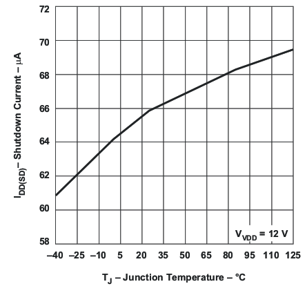 Figure 5. Shutdown Current vs Junction Temperature
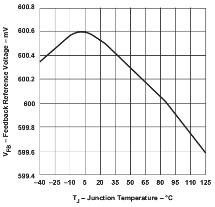 Figure 7. Feedback Reference Voltage vs Junction Temperature
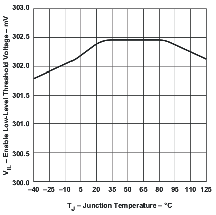 Figure 9. Enable Low-Level Threshold Voltage vs Junction Temperature
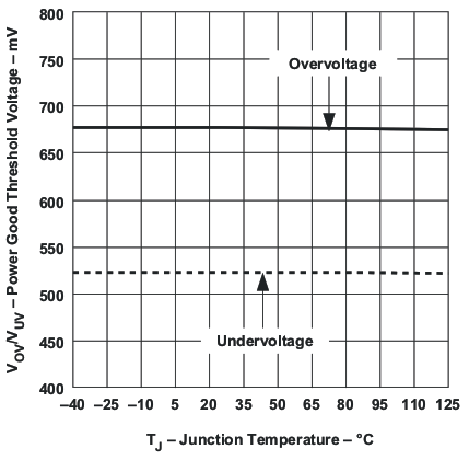 Figure 11. Power Good Threshold Voltage vs Junction Temperature
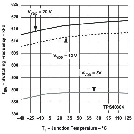 Figure 2. Switching Frequency vs Junction Temperature
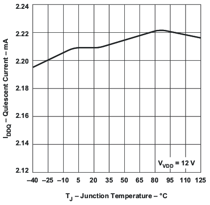 Figure 4. Quiescent Current vs Junction Temperature
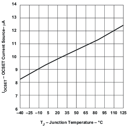 Figure 6. OCSET Current Source vs Junction Temperature
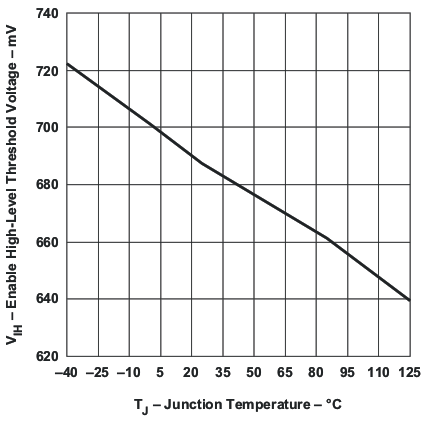 Figure 8. Enable High-Level Threshold Voltage vs Junction Temperature
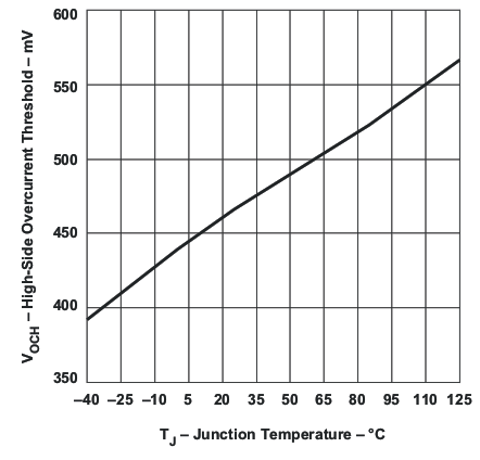 Figure 10. High-Side Overcurrent Threshold vs Junction Temperature
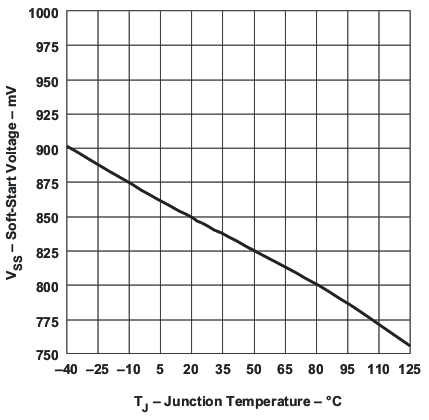 Figure 12. Soft-Start Voltage vs Junction Temperature