SLUSAF8E July 2011 – January 2016 TPS40322
PRODUCTION DATA.
- 1 Features
- 2 Applications
- 3 Description
- 4 Revision History
- 5 Pin Configuration and Functions
- 6 Specifications
-
7 Detailed Description
- 7.1 Overview
- 7.2 Functional Block Diagram
- 7.3
Feature Description
- 7.3.1 Voltage Reference
- 7.3.2 Output Voltage Setting
- 7.3.3 Input Voltage Feedforward
- 7.3.4 Current Sensing
- 7.3.5 Overcurrent Protection
- 7.3.6 Two-Phase Mode, Remote Sense Amplifier, and Current Sharing Loop
- 7.3.7 Start-Up and Shutdown
- 7.3.8 Switching Frequency and Master or Slave Synchronization
- 7.3.9 Overvoltage and Undervoltage Fault Protection
- 7.3.10 Input Undervoltage Lockout (UVLO)
- 7.3.11 Power Good
- 7.3.12 Thermal Shutdown
- 7.3.13 Connection of Unused Pins
- 7.4 Device Functional Modes
-
8 Applications and Implementation
- 8.1 Application Information
- 8.2
Typical Applications
- 8.2.1
Dual-Output Configuration from 12-V Nominal to 1.2-V and 1.8-V DC-to-DC Converter Using the TPS40322
- 8.2.1.1 Design Requirements
- 8.2.1.2
Detailed Design Procedure
- 8.2.1.2.1 Selecting a Switching Frequency
- 8.2.1.2.2 Inductor Selection (L1)
- 8.2.1.2.3 Output Capacitor Selection (C10 through C16)
- 8.2.1.2.4 Peak Current Rating of Inductor
- 8.2.1.2.5 Input Capacitor Selection (C3 through C6)
- 8.2.1.2.6 MOSFET Selection (Q1)
- 8.2.1.2.7 ILIM Resistor (R2)
- 8.2.1.2.8 Feedback Divider (R10, R14)
- 8.2.1.2.9 Compensation: (R11, R12, C17, C19, C21)
- 8.2.1.2.10 Boot-Strap Capacitor (C7)
- 8.2.1.2.11
General Device Components
- 8.2.1.2.11.1 Synchronization (SYNC Pin)
- 8.2.1.2.11.2 RT Resistor (R6)
- 8.2.1.2.11.3 Differential Amplifier Out (DIFFO Pin)
- 8.2.1.2.11.4 EN/SS Timing Capacitors (C8)
- 8.2.1.2.11.5 Power Good (PG1, PG2 Pins)
- 8.2.1.2.11.6 Phase Set (PHSET Pin)
- 8.2.1.2.11.7 UVLO Programming Resistors (R1 and R3)
- 8.2.1.2.11.8 VDD Bypass Capacitor (C2)
- 8.2.1.2.11.9 VBP6 Bypass Capacitor (C18)
- 8.2.1.3 Application Curves
- 8.2.2 Two-Phase, Single Output Configuration from 12-V nominal to 1.2-V DC-to-DC Converter Using the TPS40322
- 8.2.1
Dual-Output Configuration from 12-V Nominal to 1.2-V and 1.8-V DC-to-DC Converter Using the TPS40322
- 9 Power Supply Recommendations
- 10Layout
- 11Device and Documentation Support
- 12Mechanical, Packaging, and Orderable Information
Package Options
Mechanical Data (Package|Pins)
- RHB|32
Thermal pad, mechanical data (Package|Pins)
- RHB|32
Orderable Information
6 Specifications
6.1 Absolute Maximum Ratings
Over operating free-air temperature range, all voltages are with respect to GND (unless otherwise noted)(1)| MIN | MAX | UNIT | |||
|---|---|---|---|---|---|
| Voltage | VDD | –0.3 | 22 | V | |
| SW1, SW2 | –3 | 27 | |||
| SW1, SW2 (< 100-ns pulse width) | –5 | ||||
| SW1, SW2 (< 10-ns pulse width) | –7.5 | 30 | |||
| BOOT1, BOOT2 | –0.3 | 30 | |||
| BOOT1, BOOT2 (< 10-ns pulse width) | –0.5 | 33 | |||
| BP6 | –0.3 | 7 | |||
| HDRV1, HDRV2 | –2 | 30 | |||
| BOOT1-SW1, BOOT2-SW2, HDRV1-SW1, HDRV2-SW2 (differential from BOOT or HDRV to SW) |
–0.3 | 7 | |||
| All other pins | –0.3 | 7 | |||
| Temperature | Operating temperature, TJ | –40 | 145 | °C | |
| Storage temperature, Tstg | –55 | 150 | |||
(1) Stresses beyond those listed under Absolute Maximum Ratings may cause permanent damage to the device. These are stress ratings only, and functional operation of the device at these or any other conditions beyond those indicated under Recommended Operating Conditions is not implied. Exposure to absolute maximum rated conditions for extended periods may affect device reliability.
6.2 ESD Ratings
| VALUE | UNIT | |||
|---|---|---|---|---|
| V(ESD) | Electrostatic discharge | Human-body model (HBM), per ANSI/ESDA/JEDEC JS-001(1) | ±2000 | V |
| Charged-device model (CDM), per JEDEC specification JESD22-C101(2) | ±1500 | |||
(1) JEDEC document JEP155 states that 500-V HBM allows safe manufacturing with a standard ESD control process.
(2) JEDEC document JEP157 states that 250-V CDM allows safe manufacturing with a standard ESD control process.
6.3 Recommended Operating Conditions
| MIN | MAX | UNIT | ||
|---|---|---|---|---|
| VVDD | Input operating voltage | 3 | 20 | V |
| TJ | Operating junction temperature | –40 | 125 | °C |
6.4 Thermal Information
| THERMAL METRIC(1) | TPS40322 | UNIT | |
|---|---|---|---|
| RHB (VQFN) | |||
| 32 PINS | |||
| RθJA | Junction-to-ambient thermal resistance | 37.1 | °C/W |
| RθJC(top) | Junction-to-case (top) thermal resistance | 28.4 | °C/W |
| RθJB | Junction-to-board thermal resistance | 9.8 | °C/W |
| ψJT | Junction-to-top characterization parameter | 0.4 | °C/W |
| ψJB | Junction-to-board characterization parameter | 9.7 | °C/W |
| RθJC(bot) | Junction-to-case (bottom) thermal resistance | 2.6 | °C/W |
(1) For more information about traditional and new thermal metrics, see the Semiconductor and IC Package Thermal Metrics application report, SPRA953.
6.5 Electrical Characteristics
TJ = –40°C to 125°C, VVDD = 12 V, RRT = 40 kΩ, fSW = 500 kHz (unless otherwise noted),| PARAMETER | TEST CONDITIONS | MIN | TYP | MAX | UNIT | |
|---|---|---|---|---|---|---|
| INPUT SUPPLY | ||||||
| VDD | Input voltage range | 3 | 20 | V | ||
| IDDSDN | Shutdown | VENx/SSx = 0 V | 200 | 250 | µA | |
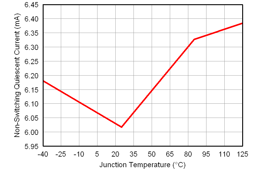
| IDDQ | Quiescent, non-switching | VFB = 0.65 V, ENx/SSx float | 6 | 8 | mA | |
| UVLO | ||||||
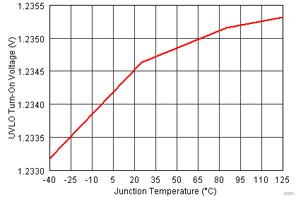
| UVLO | Minimum turn-on voltage | 1.21 | 1.24 | 1.27 | V | |
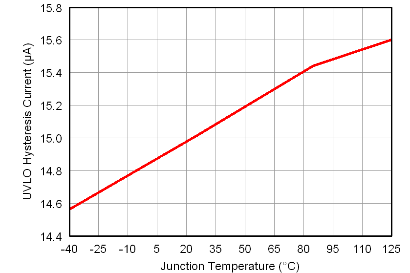
| UVLOHYS | Hysteresis current | 13 | 15 | 17 | μA | |
| BP REGULATOR | ||||||
| BP | Regulator voltage | 7 V ≤ VVDD ≤ 20 V | 6.2 | 6.5 | 6.8 | V |
| VDO | Regulator dropout voltage | IBP = 25 mA, VVDD = 3 V | 50 | 100 | mV | |
| IBP | Regulator continuous current limit(1) | 100 | mA | |||
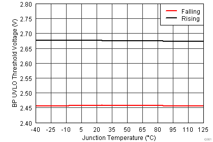
| VBPUVLO | Regulator output UVLO | 2.40 | 2.70 | 2.95 | V | |
| VBPUVLO-HYS | Regulator output UVLO hysteresis | 180 | 210 | 250 | mV | |
| OSCILLATOR AND RAMP GENERATOR | ||||||
| fSW | Oscillator frequency | 100 | 1000 | kHz | ||
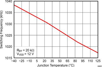
| RRT = 40 kΩ | 450 | 500 | 550 | kHz | ||
| VRAMP | Ramp amplitude (peak-to-peak) | 3 V < VVDD < 20 V | VDD / 8.5 | V | ||
| VVAL | Valley voltage | 0.85 | V | |||
| fSYNC | SYNC frequency range | 200 | 2000 | kHz | ||
| tPW(sync) | SYNC input minimum pulse width | 100 | ns | |||
| VH(sync) | Rising edge threshold to set sync pulse | 2 | V | |||
| VL(sync) | Falling edge threshold to reset sync pulse | 0.8 | V | |||
| fMASTER | Master clock frequency | 200 | 2000 | kHz | ||
| ΔfSYNC | Percent of master frequency for synchronization | –20% | 20% | |||
| VPHSET | Master | 0°/180° phase shift | 0.5 | V | ||
| Slave | 0°/180° phase shift | 0.6 | 2 | V | ||
| Slave | 90°/270° phase shift | 2.1 | V | |||
| PWM | ||||||
| PWM(off) | Minimum PWM off-time | 90 | 130 | ns | ||
| tON(min) | Minimum controllable pulse width | See (1) | 90 | ns | ||
| tDEAD | Output driver dead time | HDRV off to LDRV on | 20 | 35 | 40 | ns |
| tDEAD | Output driver dead time | LDRV off to HDRV on | 20 | 35 | 40 | ns |
| ERROR AMPLIFIER AND VOLTAGE REFERENCE | ||||||
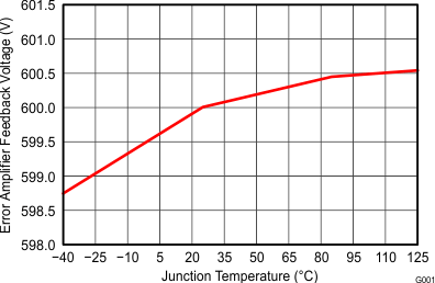
| VFB | FB input voltage | 0°C < TJ < 70°C | 597 | 600 | 603 | mV |
| –40°C < TJ < 125°C | 594 | 600 | 606 | |||
| IFB | FB input bias current | 20 | 75 | nA | ||
| GBWP | Unity gain bandwidth | See (1) | 24 | MHz | ||
| AVOL | Open loop gain | See (1) | 80 | dB | ||
| IOH | High-level output current | 3 | mA | |||
| IOL | Low-level output current | 9 | mA | |||
| ENABLE AND SOFT START | ||||||
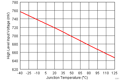
| VIH | High-level input voltage | 0.55 | 0.7 | 1 | V | |
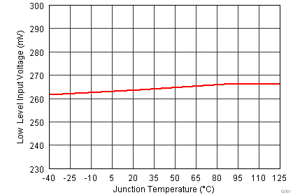
| VIL | Low-level input voltage | 0.23 | 0.26 | 0.3 | V | |
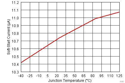
| ISS | Soft-start source current | 8 | 10 | 12 | μA | |
| VSS | Soft-start voltage level | 0.8 | V | |||
| IDISCHG | Soft-start discharge current | 130 | μA | |||
| OVERCURRENT PROTECTION | ||||||
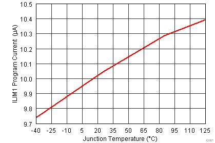
| IILIM | ILIM program current | TJ = 25°C | 9.5 | 10 | 10.5 | μA |
| tHICCUP | Hiccup cycles to recover | 6 | Cycles | |||
| CURRENT SENSE AMPLIFIER | ||||||
| VDIFF | Differential input voltage range | –60 | 60 | mV | ||
| VCM | Input common mode range | 0 | 5.6 | V | ||
| ACS | Current sensing gain | 15 | V/V | |||
| VCSOUT | Current sense amplifier output | VCSIN = 20 mV, TJ = 25°C | 270 | 300 | 330 | mV |
| fC0 | Closed loop bandwidth(1) | 3 | MHz | |||
| Current sense amplifier output difference between CH1 and CH2 | VCSIN = 20 mV to both CS1 and CS2 | –15 | 15 | mV | ||
| OVERVOLTAGE AND UNDERVOLTAGE PROTECTION | ||||||
| VOVP | Feedback voltage limit for OVP | 679 | 700 | 735 | mV | |
| VUVP | Feedback voltage limit for UVP | 475 | 500 | 525 | mV | |
| GATE DRIVERS | ||||||
| RHDHI | High-side driver pull-up resistance | VBOOT – VSW = 6.5 V, IHDRV = –40 mA | 0.8 | 1.5 | 2.5 | Ω |
| RHDLO | High-side driver pull-down resistance | VBOOT – VSW = 6.5 V, IHDRV = 40 mA | 0.5 | 1 | 1.6 | Ω |
| RLDHI | Low-side driver pull-up resistance | ILDRV = –40 mA | 0.8 | 1.5 | 2.5 | Ω |
| RLDLO | Low-side driver pull-down resistance | ILDRV = 40 mA | 0.35 | 0.6 | 1.3 | Ω |
| tHRISE | High-side driver rise time | CLOAD = 5 nF, See (1) | 15 | ns | ||
| tHFALL | High-side driver fall time | CLOAD = 5 nF, See (1) | 12 | ns | ||
| tLRISE | Low-side driver rise time | CLOAD = 5 nF, See (1) | 15 | ns | ||
| tLFALL | Low-side driver fall time | CLOAD = 5 nF, See(1) | 10 | ns | ||
| BOOT SWITCH | ||||||
| VDFWD | Bootstrap switch voltage drop | IBOOT = 5 mA | 0.1 | V | ||
| REMOTE SENSE | ||||||
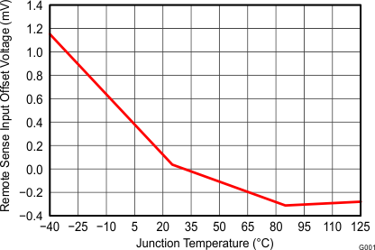
| VIOFSET | Input offset voltage | VDIFFO = 0.9 V | –2 | 2 | mV | |
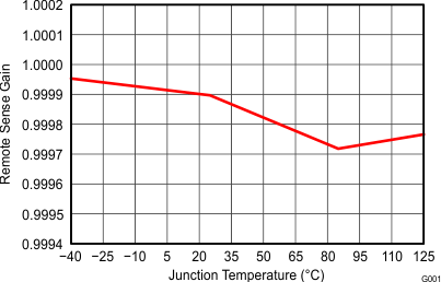
| Gain | Differential gain | 0.995 | 1.005 | V/V | ||
| BW | Close loop bandwidth(1) | 2 | MHz | |||
| VDIFFO | Output voltage at DIFFO pin | VBP6 – 0.2 | V | |||
| ISRC | Output source current | 1 | mA | |||
| ISNK | Output sink current | 1 | mA | |||
| POWERGOOD | ||||||
| VOV | Feedback voltage limit for PGOOD | 650 | 675 | 697 | mV | |
| VUV | Feedback voltage limit for PGOOD | 510 | 525 | 545 | mV | |
| VPGD(hyst) | PGOOD hysteresis voltage at FB | 25 | 40 | mV | ||
| RRGD | PGOOD pull down resistance | 50 | 70 | Ω | ||
| IPGD(leak) | PGOOD leakage current | 20 | µA | |||
| THERMAL SHUTDOWN | ||||||
| TSD | Junction shutdown temperature | See (1) | 150 | °C | ||
| TSD(hyst) | Hysteresis | See (1) | 20 | °C | ||
(1) Specified by design. Not production tested.
6.6 Typical Characteristics
