SLUSAF8E July 2011 – January 2016 TPS40322
PRODUCTION DATA.
- 1 Features
- 2 Applications
- 3 Description
- 4 Revision History
- 5 Pin Configuration and Functions
- 6 Specifications
-
7 Detailed Description
- 7.1 Overview
- 7.2 Functional Block Diagram
- 7.3
Feature Description
- 7.3.1 Voltage Reference
- 7.3.2 Output Voltage Setting
- 7.3.3 Input Voltage Feedforward
- 7.3.4 Current Sensing
- 7.3.5 Overcurrent Protection
- 7.3.6 Two-Phase Mode, Remote Sense Amplifier, and Current Sharing Loop
- 7.3.7 Start-Up and Shutdown
- 7.3.8 Switching Frequency and Master or Slave Synchronization
- 7.3.9 Overvoltage and Undervoltage Fault Protection
- 7.3.10 Input Undervoltage Lockout (UVLO)
- 7.3.11 Power Good
- 7.3.12 Thermal Shutdown
- 7.3.13 Connection of Unused Pins
- 7.4 Device Functional Modes
-
8 Applications and Implementation
- 8.1 Application Information
- 8.2
Typical Applications
- 8.2.1
Dual-Output Configuration from 12-V Nominal to 1.2-V and 1.8-V DC-to-DC Converter Using the TPS40322
- 8.2.1.1 Design Requirements
- 8.2.1.2
Detailed Design Procedure
- 8.2.1.2.1 Selecting a Switching Frequency
- 8.2.1.2.2 Inductor Selection (L1)
- 8.2.1.2.3 Output Capacitor Selection (C10 through C16)
- 8.2.1.2.4 Peak Current Rating of Inductor
- 8.2.1.2.5 Input Capacitor Selection (C3 through C6)
- 8.2.1.2.6 MOSFET Selection (Q1)
- 8.2.1.2.7 ILIM Resistor (R2)
- 8.2.1.2.8 Feedback Divider (R10, R14)
- 8.2.1.2.9 Compensation: (R11, R12, C17, C19, C21)
- 8.2.1.2.10 Boot-Strap Capacitor (C7)
- 8.2.1.2.11
General Device Components
- 8.2.1.2.11.1 Synchronization (SYNC Pin)
- 8.2.1.2.11.2 RT Resistor (R6)
- 8.2.1.2.11.3 Differential Amplifier Out (DIFFO Pin)
- 8.2.1.2.11.4 EN/SS Timing Capacitors (C8)
- 8.2.1.2.11.5 Power Good (PG1, PG2 Pins)
- 8.2.1.2.11.6 Phase Set (PHSET Pin)
- 8.2.1.2.11.7 UVLO Programming Resistors (R1 and R3)
- 8.2.1.2.11.8 VDD Bypass Capacitor (C2)
- 8.2.1.2.11.9 VBP6 Bypass Capacitor (C18)
- 8.2.1.3 Application Curves
- 8.2.2 Two-Phase, Single Output Configuration from 12-V nominal to 1.2-V DC-to-DC Converter Using the TPS40322
- 8.2.1
Dual-Output Configuration from 12-V Nominal to 1.2-V and 1.8-V DC-to-DC Converter Using the TPS40322
- 9 Power Supply Recommendations
- 10Layout
- 11Device and Documentation Support
- 12Mechanical, Packaging, and Orderable Information
Package Options
Mechanical Data (Package|Pins)
- RHB|32
Thermal pad, mechanical data (Package|Pins)
- RHB|32
Orderable Information
7 Detailed Description
7.1 Overview
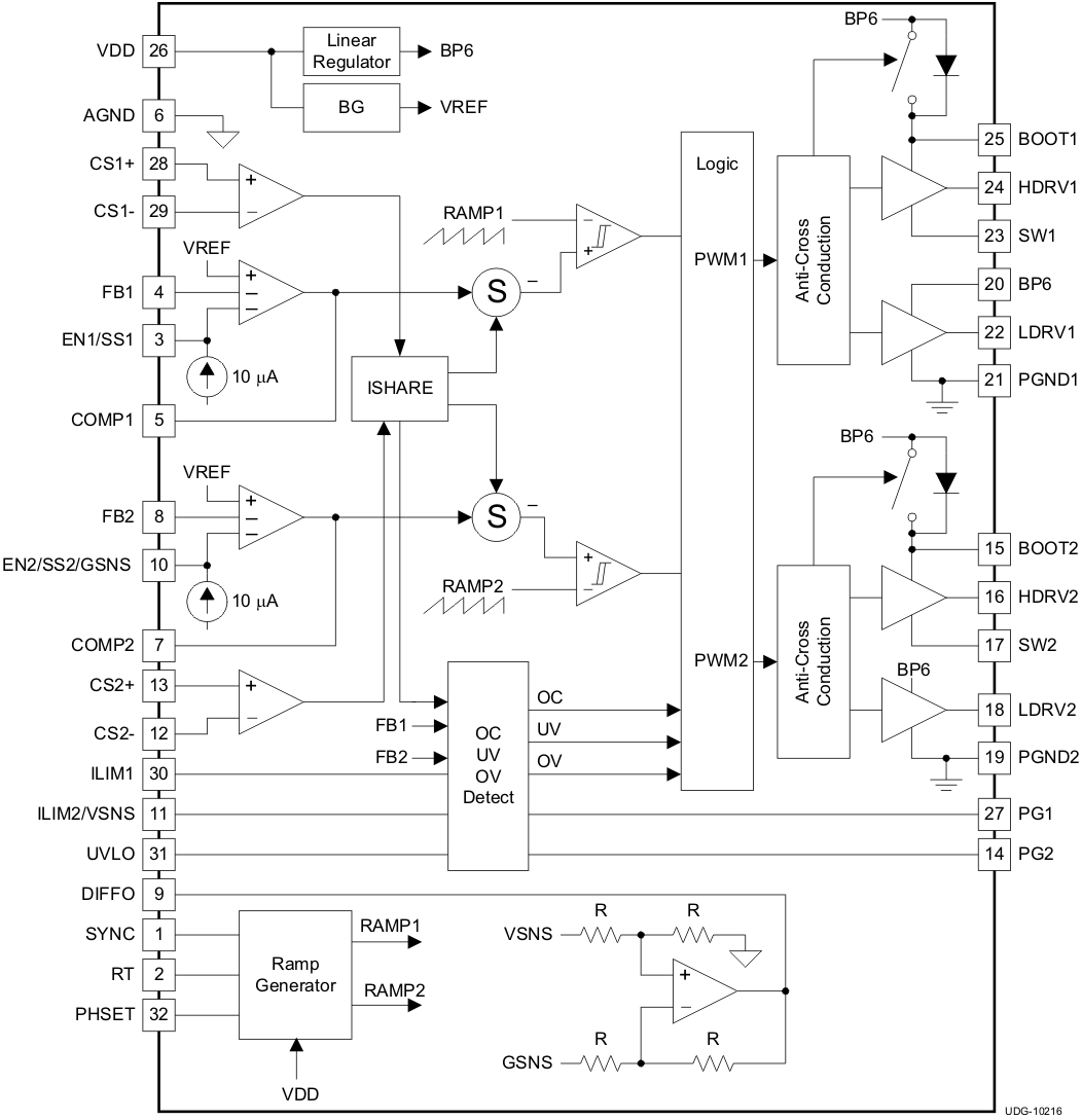
The TPS40322 is a flexible synchronous buck controller. It can be used as a dual-output controller, or as a two-phase, single-output controller. It operates with a wide input range from 3 V to 20 V and can generate an accurate regulated output as low as 600 mV.
In dual output mode, voltage mode control with input feedforward architecture is implemented. With this architecture, the benefits are less noise sensitivity, no control instability issues for small DCR applications, and a smaller minimum controllable on-time, often desired for high conversion ratio applications.
In two-phase, single-output mode, a current-sharing loop is implemented to ensure a balance of current between phases. Because the induced error current signal to the loop is much smaller when compared to the PWM ramp amplitude, the control loop is modeled as voltage mode with input feedforward.
DESIGN NOTE
When the device is operating in dual output mode, DIFFO must be floating or tied to BP6.
7.3 Feature Description
7.3.1 Voltage Reference
The 600-mV band gap cell is internally connected to the non-inverting input of the error amplifier. The reference voltage is trimmed with the error amplifier in a unity gain configuration to remove amplifier offset from the final regulation voltage. The 0.5% tolerance on the reference voltage allows the user to design a very accurate power supply.
7.3.2 Output Voltage Setting
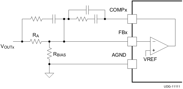
The output voltages of the TPS40322 are set by using external feedback resistor dividers as shown in Figure 15. The regulated output voltage (VOUT) is determined by Equation 1.

7.3.3 Input Voltage Feedforward
The TPS40322 uses input voltage feedforward to maintain a constant power stage gain as the input voltage varies and provides very good response to input voltage transient disturbances. The simple constant power stage gain of the controller greatly simplifies feedback loop design because the loop characteristics remain constant as the input voltage changes, unlike a typical buck converter without voltage feedforward. For modeling purposes, the gain from the COMP pin to the average voltage at the input of the L-C filter is typically 8.5 V/V.
7.3.4 Current Sensing
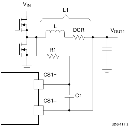
The TPS40322 uses a differential current sense design to sense the output current. The sense element can be the series resistance of the power stage filter inductor or a separate current sense resistor. When using the inductor series resistance as shown in Figure 16, an R-C filter must be used to remove the large AC component voltage across the inductor so that only the component of the voltage that remains is across the resistance of the inductor (see Figure 16).
The values of R1 and C1 for an ideal design can be calculated using Equation 2. The time constant of the R-C filter must equal the time constant of the inductor itself. If the time constants are equal, the voltage across C1 equals the current in the inductor multiplied by the inductor resistance. The inductor ripple current is reflected in the voltage across C1. Typically a capacitor with a value of 0.1-µF is recommended for C1.
Refer to the Layout section for proper placement of the sensing elements.

7.3.5 Overcurrent Protection
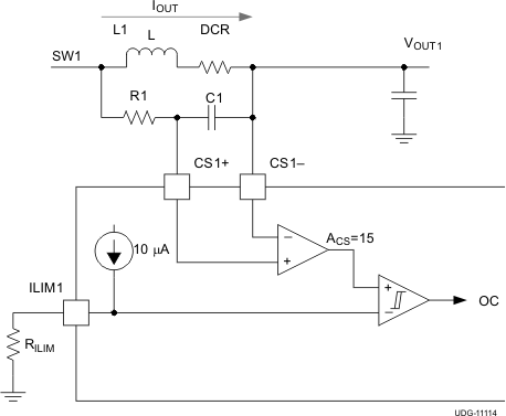
The TPS40322 has dedicated ILIM pins for each channel for use when operating in dual-output mode. When operating in two-phase mode, both channels share the same overcurrent level set by ILIM1. The overcurrent level is set with a resistor connected from the ILIMx pin to analog ground. The sensed current signal is amplified by the CS amplifier with a gain of 15, and then compared with the established overcurrent level to determine if there is an OC fault. This design is shown in Figure 17.
Equation 3 is the current limit resistance (RLIM) calculation for desired overcurrent limit.

where
- IOC is the desired DC over current limit level
- IRIPPLE is the inductor peak-peak ripple current
- DCR is the inductor DC resistance
- ACS is the current sensing amplifier gain (typically 15)
- IILIM is the internal source current out of ILIMx pin (typically 10 µA)
The TPS40322 implements cycle-by-cycle current limit when the inductor peak current has exceeded the set limit. When the controller counts three consecutive clock cycles of an overcurrent condition, the high-side and low-side MOSFETs are turned off and the controller enters a hiccup mode. After six soft-start cycles, normal switching is attempted. If the overcurrent has cleared, normal operation resumes, otherwise the sequence repeats.
7.3.6 Two-Phase Mode, Remote Sense Amplifier, and Current Sharing Loop
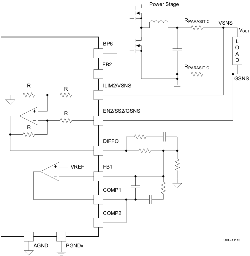
The TPS40322 can be configured to operate in single-output, two-phase mode for high-current applications. With proper selection of the external MOSFETs, this device can support up to 50-A of load current in a two-phase configuration. As shown in Figure 18, to configure the TPS40322 for two-phase mode, FB2 is tied to BP6. In this mode, COMP1 must be connected to COMP2 to ensure current sharing between the two phases. For high-current applications, the remote sense amplifier is used to compensate for the parasitic offset to provide an accurate output voltage. The EN2/SS2 and ILIM2 pins are designed for multiple functions. They are used as VSNS and GSNS for remote sensing in two-phase mode. DIFFO, which is the output of the remote sensing amplifier, is connected to the resistor divider of the feedback network.
Note that BP6 powers the remote sense amplifier. The DIFFO voltage must be 0.2-V lower than the BP6 voltage under all conditions. If BP6 is lower than DIFFO voltage, the converter loses regulation. To ensure no regulation loss, use a remote sense amplifier when the application output voltage is lower than 2.2 V. For an application in which the output voltage is higher than 2.2 V, the remote sense amplifier can be bypassed and the voltage output can be connected to the feedback resistor divider directly.
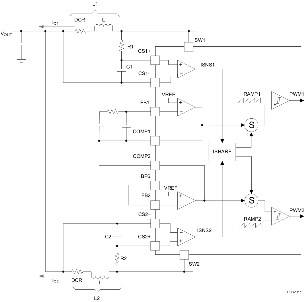
When the device operates in two-phase mode, a current sharing loop as shown in Figure 19 is designed to maintain the current balance between phases. Both phases share the same comparator voltage (COMP1). The sensed current from each phase is compared first in a current share block, then each signal is summed with COMP. The resulted error voltage is compared with the voltage ramp to generate the PWM pulse for each channel.
7.3.7 Start-Up and Shutdown
7.3.7.1 Start-Up Sequence
When the ENx/SSx pin is pulled below 0.3 V, the respective channel is disabled. When ENx/SSx is released, the controller starts automatically and an internal 40-µA current source begins to charge the external soft-start capacitor. When the voltage across the soft-start capacitor is over 0.7 V, the internal BP regulator is enabled. The ENx/SSx voltage is clamped to 1.3 V while waiting for signals indicating that BP6, VDD, and the oscillator clock are good. After all the signals are confirmed, ENx/SSx is discharged to 0.4 V with a 140-µA current source, and then charged again with the internal 10-µA current source. The operation is described by the waveform shown in Figure 20. VSS_INT is an internal signal level shifted from ENx/SSx and then connected to the non-inverting terminal of the error amplifier.
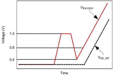 Figure 20. EN/SS Start-Up Waveform
The soft-start time is determined by the internal charge current and the external capacitance. The actual output ramp-up time is the time for the internal current source to charge the capacitor through a 600-mV range. There is some initial lag time due to the offset (800 mV typical) from the actual ENx/SSx pin voltage to VSS_INT. The soft-start sequence takes place in a closed loop fashion, meaning that the error amplifier controls the output voltage constantly during the soft-start period and the feedback loop is never open (as occurs in duty cycle limit soft-start designs). The error amplifier has two non-inverting inputs, one connected to the 600-mV reference voltage, and the other connected to the offset VSS_INT. The error amplifier controls the FB pin to the lower of these two voltages. As the voltage on the ENx/SSx pin ramps up past approximately 1.4 V (800-mV offset voltage plus the 600-mV reference voltage), the 600-mV reference voltage becomes the dominant input and the converter has reached its final regulation voltage.
Equation 4 is the calculation for soft-start capacitance.

where
- CSS is the soft-start capacitance connected to ENx/SSx pin
- tSS is the desired soft-start time
- ISS is the internal soft-start current (typically 10 µA)
7.3.7.2 Prebiased Output Start-Up
The TPS40322 contains a circuit that prevents current from being pulled from the output during the start-up sequence in a pre-biased output condition. There are no PWM pulses until the internal soft-start voltage rises above the error amplifier input (FBx pin), if the output is pre-biased. Once the soft-start voltage exceeds the error amplifier input, the device slowly initiates synchronous rectification by starting the synchronous rectifier with a narrow on-time. It then increments that on-time on a cycle-by-cycle basis until it coincides with the time dictated by (1-D), where D is the duty cycle of the converter. This approach prevents the sinking of current from a pre-biased output, and ensures the output voltage start-up and ramp-to-regulation sequences are smooth and controlled.
DESIGN NOTE
During the soft-start sequence, when the PWM pulse width is shorter than the minimum controllable on-time, which is generally caused by the PWM comparator and gate driver delays, pulse skipping may occur and the output might show larger ripple voltage.
7.3.7.3 Shutdown
During the shutdown sequence, BP6 is controlled by ENx/SSx. If both of ENx/SSx pins are pulled low, BP6 is turned off regardless of the input voltage remaining higher than the programmed UVLO threshold.
7.3.8 Switching Frequency and Master or Slave Synchronization
The switching frequency is set by the value of the resistor connected from the RT pin to AGND. The RT resistor value is calculated in Equation 5.

where
- RRT is the the resistor from RT pin to AGND, in Ω
- fSW is the desired switching frequency, in Hz
The TPS40322 device can also synchronize to an external clock that is ±20% of the master clock frequency which is two times the free running frequency. Each TPS40322 can be set by the PHSET pin as either master or slave. The master produces a 50% duty cycle clock to the slave. The slave synchronizes to the external clock with 50% duty cycle and selects the phase shift angle as shown in Table 1.
Figure 21 shows an example of synchronizing two TPS40322 devices to generate an evenly distributed shift to reduce input ripple.
Table 1. Phase Shift Angle Selection
| PHSET | MODE | PHASE ANGLE (°) | ||
|---|---|---|---|---|
| CONNECTION | RANGE (V) |
CH1 | CH2 | |
| AGND | < 0.5 | Master | 0 | 180 |
| Floating | 0.6 to 2 | Slave | 0 | 180 |
| High | > 2.1 | Slave | 90 | 270 |
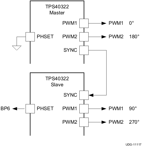 Figure 21. Synchronizing Two TPS40322 Devices
7.3.9 Overvoltage and Undervoltage Fault Protection
The TPS40322 has output overvoltage protection and undervoltage protection capability. The comparators that regulate the overvoltage and undervoltage conditions use the FBx pin as the output sensing point so the filtering effect of the compensation network connected from COMPx to FBx has an effect on the speed of detection. As the output voltage rises or falls below the nominal value, the error amplifier attempts to force FBx to match its reference voltage. When the error amplifier is no longer able to do this, the FB pin begins to drift and trip the overvoltage threshold (VOVP) or the undervoltage threshold (VUVP) as described in the Electrical Characteristics table.
When an undervoltage fault is detected, the TPS40322 enters hiccup mode and resumes normal operation when the fault is cleared.
When an overvoltage fault is detected, the TPS40322 turns off the high-side MOSFET and latches on the low-side MOSFET to discharge the output current to the regulation level (within the Power Good window).
When operating in dual-channel mode, both channels have identical yet independent protection schemes, which means one channel is not affected when the other channel is in fault mode.
When operating in two-phase mode, only the FB1 pin is detected for overvoltage and undervoltage fault. Therefore both channels take action together during a fault.
7.3.10 Input Undervoltage Lockout (UVLO)
A dedicated UVLO pin allows the user to program the desired input turn-on threshold voltage. The diagram is shown in Figure 22. The desired input turn-on threshold can be calculated using Equation 6. The input turn off hysteresis can be calculated using Equation 7.
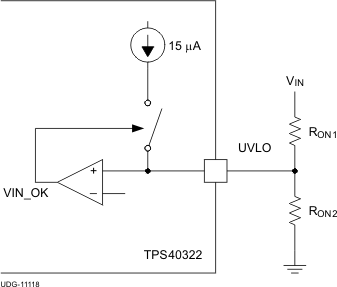 Figure 22. Input UVLO Diagram


7.3.11 Power Good
The TPS40322 provides an indication that output is good for each channel. This is an open-drain signal that pulls low when any condition exists that would indicate that the output of the supply might be out of regulation. These conditions include:
- Feedback voltage (VFB) is more than ±12.5% from nominal
- Soft-start is active
7.3.12 Thermal Shutdown
If the junction temperature of the device reaches the thermal shutdown limit of 150°C, the PWMs and the oscillators are turned off and HDRVs and LDRVs are driven low. When the junction cools to the required level (130°C typical), the PWM initiates soft start as during a normal power-up cycle.
7.3.13 Connection of Unused Pins
In some case, it is possible that some pins are not used. For example, if only channel 1 is used, then pins for channel 2 need to be properly connected as well. The unused pin connections are summarized in Table 2.
Table 2. Unused Pin Connections
| PIN NAME | CONNECTION | |||
|---|---|---|---|---|
| BOOTx | Floating | |||
| COMPx | Floating | |||
| CSx– | Connect to a voltage between 0 V and 5.6 V, short to CSx+ | |||
| CSx+ | Short to CSx- | |||
| DIFFO | Floating | |||
| EN1/SS1 | Connect to ground | |||
| EN2/SS2/GSNS | Connect to ground | |||
| FBx | Connect to ground | |||
| HDRVx | Floating | |||
| ILIM1 | Connect to ground through a 100-kΩ resistor | |||
| ILIM2/VSNS | Connect to ground through a 100-kΩ resistor | |||
| LDRVx | Floating | |||
| PGx | Connect to ground | |||
| PHSET | Connect to ground | |||
| SWx | Connect to ground | |||
| SYNCx | Floating | |||
7.4 Device Functional Modes
At dual-output configuration, EN1/SS1 and EN2/SS2/GSNS pins are used to enable or disable switching of channel 1 and channel 2, respectively. Floating the pin turns the channel on, pulling the pin low turns the channel off. At two-phase configuration, EN1/SS1 pin is used to enable and disable switching of both channels.
