SLVSA82F March 2011 – December 2014 TPS43330-Q1 , TPS43332-Q1
PRODUCTION DATA.
- 1 Features
- 2 Applications
- 3 Description
- 4 Revision History
- 5 Device Comparison Table
- 6 Pin Configuration and Functions
- 7 Specifications
-
8 Detailed Description
- 8.1 Overview
- 8.2 Functional Block Diagram
- 8.3 Feature Description
- 8.4 Device Functional Modes
-
9 Application and Implementation
- 9.1 Application Information
- 9.2
Typical Application
- 9.2.1 Design Requirements
- 9.2.2
Detailed Design Procedure
- 9.2.2.1 Boost Component Selection
- 9.2.2.2 Boost Maximum Input Current IIN_MAX
- 9.2.2.3 Boost Inductor Selection, L
- 9.2.2.4 Inductor Ripple Current, IRIPPLE
- 9.2.2.5 Peak Current in Low-Side FET, IPEAK
- 9.2.2.6 Right Half-Plane Zero RHP Frequency, fRHP
- 9.2.2.7 Output Capacitor, COUTx
- 9.2.2.8 Bandwidth of Boost Converter, fC
- 9.2.2.9 Output Ripple Voltage Due to Load Transients, ∆VOUTx
- 9.2.2.10 Selection of Components for Type II Compensation
- 9.2.2.11 Input Capacitor, CIN
- 9.2.2.12 Output Schottky Diode D1 Selection
- 9.2.2.13 Low-Side MOSFET (BOT_SW3)
- 9.2.2.14 BuckA Component Selection
- 9.2.2.15 Inductor Selection L
- 9.2.2.16 Inductor Ripple Current IRIPPLE
- 9.2.2.17 Output Capacitor COUTA
- 9.2.2.18 Bandwidth of Buck Converter fC
- 9.2.2.19 Selection of Components for Type II Compensation
- 9.2.2.20 Resistor Divider Selection for Setting VOUTA Voltage
- 9.2.2.21 BuckB Component Selection
- 9.2.2.22 Resistor Divider Selection for Setting VOUT Voltage
- 9.2.2.23 BuckX High-Side and Low-Side N-Channel MOSFETs
- 9.2.3 Application Curves
- 10Power Supply Recommendations
- 11Layout
- 12Device and Documentation Support
- 13Mechanical, Packaging, and Orderable Information
Package Options
Mechanical Data (Package|Pins)
- DAP|38
Thermal pad, mechanical data (Package|Pins)
- DAP|38
Orderable Information
9 Application and Implementation
NOTE
Information in the following applications sections is not part of the TI component specification, and TI does not warrant its accuracy or completeness. TI’s customers are responsible for determining suitability of components for their purposes. Customers should validate and test their design implementation to confirm system functionality.
9.1 Application Information
The TPS43330-Q1 and TPS43332-Q1 devices are ideally suited as a pre-regulator stage with low Iq requirements and for applications that must survive supply drops due to cranking events. The integrated boost controller allows the devices to operate down to 2 V at the input without seeing a drop on the buck regulator output stages. Below component values and calculations are a good starting point and theoretical representation of the values for use in the application; improving the performance of the device may require further optimization of the derived components.
9.2 Typical Application
The following example illustrates the design process and component selection for the TPS43330-Q1 device.
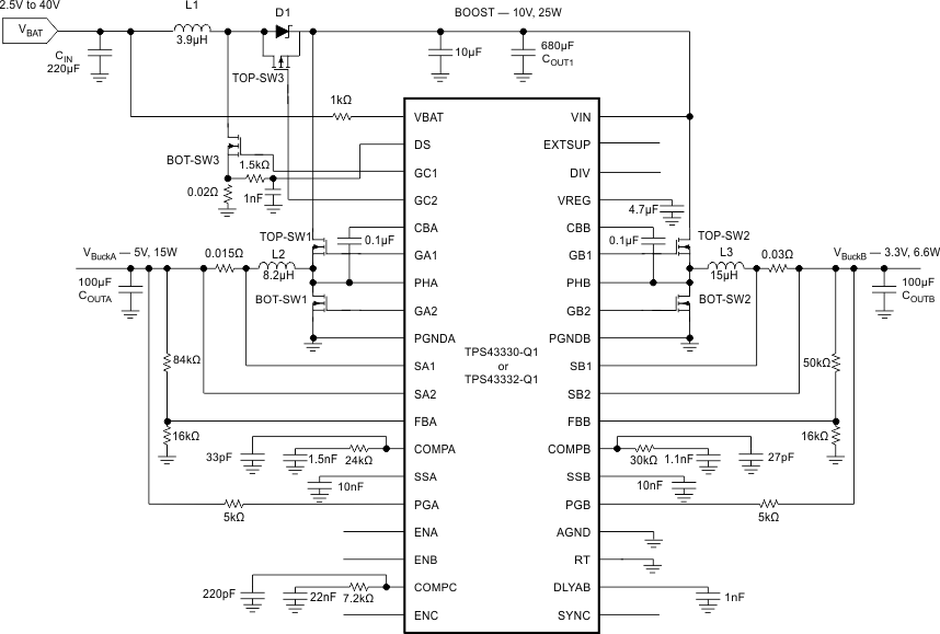 Figure 22. Simplified Application Schematic
9.2.1 Design Requirements
Table 3 lists the design-goal parameters.
Table 3. Application Example
| PARAMETER | VBuckA | VBuckB | BOOST |
|---|---|---|---|
| Input voltage | VIN = 6 V to 30 V 12 V - typical |
VIN = 6 V to 30 V 12 V - typical |
VBAT = 5 V (cranking pulse input) to 30 V |
| Output voltage, VOUTx | 5 V | 3.3 V | 10 V |
| Maximum output current, IOUTx | 3 A | 2 A | 2.5 A |
| Load-step output tolerance, ∆VOUT + ∆VOUT(Ripple) | ±0.2 V | ±0.12 V | ±0.5 V |
| Current output load step, ∆IOUTx | 0.1 A to 3 A | 0.1 A to 2 A | 0.1 A to 2.5 A |
| Converter switching frequency, fSW | 400 kHz | 400 kHz | 200 kHz |
9.2.2 Detailed Design Procedure
The component values for this design example are calculated using the same equations as used for above example. In this example, the boost operates at 150 kHz , while the buck operates at 300 kHz each. The Buck A operates down to 5 V to give.
Table 4. Application Example – Component Proposals
| NAME | COMPONENT PROPOSAL | VALUE |
|---|---|---|
| L1 | MSS1278T-392NL (Coilcraft) | 4 µH |
| L2 | MSS1278T-822ML (Coilcraft) | 8.2 µH |
| L3 | MSS1278T-153ML (Coilcraft) | 15 µH |
| D1 | SK103 (Micro Commercial Components) | |
| TOP_SW3 | IRF7416 (International Rectifier) | |
| TOP_SW1, TOP_SW2 | Si4840DY-T1-E3 (Vishay) | |
| BOT_SW1, BOT_SW2 | Si4840DY-T1-E3 (Vishay) | |
| BOT_SW3 | IRFR3504ZTRPBF (International Rectifier) | |
| COUT1 | EEVFK1J681M (Panasonic) | 680 µF |
| COUTA, COUTB | ECASD91A107M010K00 (Murata) | 100 µF |
| CIN | EEEFK1V331P (Panasonic) | 220 µF |
9.2.2.1 Boost Component Selection
A boost converter operating in continuous-conduction mode (CCM) has a right-half-plane (RHP) zero in its transfer function. The RHP zero relates inversely to the load current and inductor value and directly to the input voltage. The RHP zero limits the maximum bandwidth achievable for the boost regulator. If the bandwidth is too close to the RHP zero frequency, the regulator may become unstable.
Thus, for high-power systems with low input voltages, choose a low inductor value. A low value increases the amplitude of the ripple currents in the N-channel MOSFET, the inductor, and the capacitors for the boost regulator. Select these components with the ripple-to-RHP zero trade-off in mind and considering the power dissipation effects in the components because of parasitic series resistance.
A boost converter that operates always in the discontinuous mode does not contain the RHP zero in the transfer function. However, designing for the discontinuous mode demands an even lower inductor value that has high ripple currents. Also, ensure that the regulator never enters the continuous-conduction mode; otherwise, it can become unstable.
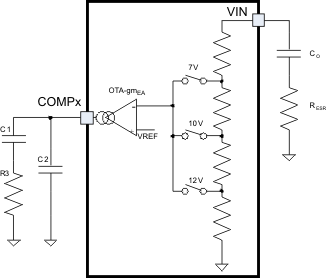 Figure 23. Boost Compensation Components
This design assumes operation in continuous-conduction mode. During light load conditions, the boost converter operates in discontinuous mode without affecting stability. Hence, the assumptions here cover the worst case for stability.
9.2.2.2 Boost Maximum Input Current IIN_MAX
The maximum input current flows at the minimum input voltage and maximum load. The efficiency for VBAT = 5 V at 2.5 A is 80%, based on the graphs in the Typical Characteristicssection.
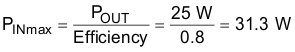
Therefore:
9.2.2.3 Boost Inductor Selection, L
Allow an input ripple current of 40% of IIN max at VBAT = 5 V.
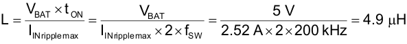
Select a lower value of 4 µH to ensure a high RHP-zero frequency while making a compromise that expects a high current ripple. This inductor selection also makes the boost converter operate in discontinuous conduction mode, where compensation is easier.
The inductor saturation current must be higher than the peak inductor current and some percentage higher than the maximum current-limit value set by the external resistive sensing element.
Determine the saturation rating at the minimum input voltage, maximum output current, and maximum core temperature for the application.
9.2.2.4 Inductor Ripple Current, IRIPPLE
Based on an inductor value of 4 µH, the ripple current is approximately 3.1 A.
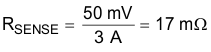
9.2.2.5 Peak Current in Low-Side FET, IPEAK

Based on this peak current value, calculate the external current-sense resistor, RSENSE.
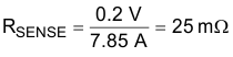
Select 20 mΩ, allowing for tolerance.
The filter component values RIFLT and CIFLT for current sense are 1.5 kΩ and 1 nF, respectively, which allows for good noise immunity.
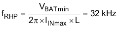
9.2.2.6 Right Half-Plane Zero RHP Frequency, fRHP
9.2.2.7 Output Capacitor, COUTx
To ensure stability, select the output capacitor, COUTx, such that Equation 11 is true.
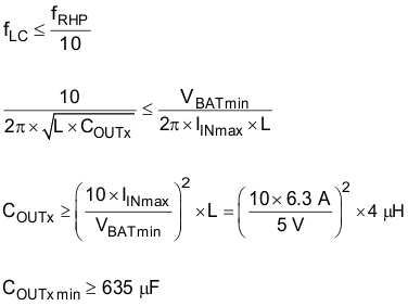
Select COUTx = 680 µF.
This capacitor is usually aluminum electrolytic with ESR in the tens of milliohms. ESR in this range is good for loop stability, because it provides a phase boost. The output filter components, L and C, create a double pole (180-degree phase shift) at a frequency fLC and the ESR of the output capacitor RESR creates a zero for the modulator at frequency fESR. Use Equation 12 to determine these frequencies.
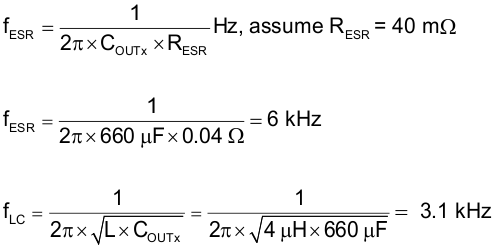
Equation 12 satisfies fLC ≤ 0.1 fRHP.
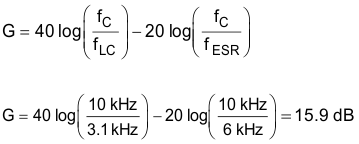
9.2.2.8 Bandwidth of Boost Converter, fC
Use the following guidelines to set the frequency poles, zeroes, and crossover values for the trade-off between stability and transient response:
9.2.2.9 Output Ripple Voltage Due to Load Transients, ∆VOUTx
Assume a bandwidth of fC = 10 kHz.
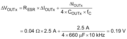
Because the boost converter is active only during brief events such as a cranking pulse, and the buck converters are high-voltage tolerant, a higher excursion on the boost output may be tolerable in some cases. In such cases, select smaller components for the boost output.
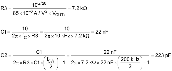
9.2.2.10 Selection of Components for Type II Compensation
The required loop gain for unity-gain bandwidth (UGB) is calculated with Equation 14.
The boost-converter error amplifier (OTA) has a Gm that is proportional to the VBAT voltage. This Gm allows a constant loop response across the input-voltage range and makes compensation easier by removing the dependency on VBAT.
9.2.2.11 Input Capacitor, CIN
The input ripple required is lower than 50 mV.
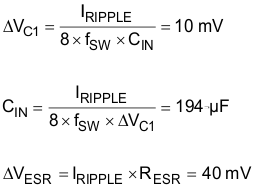
Therefore, TI recommends 220 µF with 10-mΩ ESR.
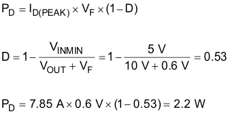
9.2.2.12 Output Schottky Diode D1 Selection
Maximizing efficiency requires a Schottky diode with low forward-conducting voltage, VF, over temperature and fast switching characteristics. The reverse breakdown voltage should be higher than the maximum input voltage, and the component should have low reverse leakage current. Additionally, the peak forward current should be higher than the peak inductor current. The following calculation gives the power dissipation in the Schottky diode:
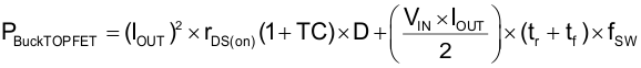
9.2.2.13 Low-Side MOSFET (BOT_SW3)
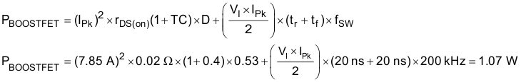
The times tr and tf denote the rising and falling times of the switching node and relate to the gate-driver strength of the TPS43330-Q1 device, TPS43332-Q1 device, and gate Miller capacitance of the MOSFET. The first term denotes the conduction losses, which the low on-resistance of the MOSFET minimizes. The second term denotes the transition losses which arise because of the full application of the input voltage across the drain-source of the MOSFET as it turns on or off. Transition losses are higher at high output currents and low input voltages (because of the large input peak current) and when the switching time is low.
NOTE
The on-resistance, rDS(on), has a positive temperature coefficient, which produces the
(TC = d × ΔT) term that signifies the temperature dependence. (Temperature coefficient d is available as a normalized value from MOSFET data sheets and can have an assumed starting value of 0.005 per °C.)
9.2.2.14 BuckA Component Selection
9.2.2.14.1 BuckA Component Selection

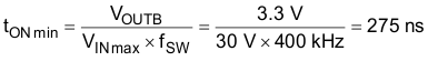
tON min is higher than the minimum duty cycle specified (100 ns typical). Hence, the minimum duty cycle is achievable at this frequency.
9.2.2.14.2 Current-Sense Resistor RSENSE
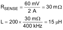
Based on the typical characteristics for the VSENSE limit with VIN versus duty cycle, the sense limit is approximately 65 mV (at VIN = 12 V and duty cycle of 5 V / 12 V = 0.416). Allowing for tolerances and ripple currents, select a VSENSE maximum of 50 mV.
Select a value of 15 mΩ for RSENSE.
9.2.2.15 Inductor Selection L
As explained in the description of the buck controllers, for optimal slope compensation and loop response, choose the inductor such that:
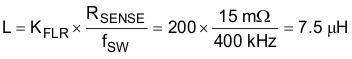
KFLR = coil-selection constant = 200
Select a standard value of 8.2 µH. For the buck converter, select the inductor saturation currents and core to sustain the maximum currents.
9.2.2.16 Inductor Ripple Current IRIPPLE
At the nominal input voltage of 12 V, this inductor value causes a ripple current of 30% of IOUT max ≈ 1 A.
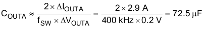
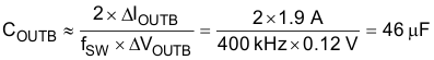
9.2.2.17 Output Capacitor COUTA
Select an output capacitance COUTA of 100 µF with low ESR in the range of 10 mΩ, giving ∆VOUT(Ripple) ≈ 15 mV and a ∆V drop of ≈ 180 mV during a load step, which does not trigger the power-good comparator and is within the required limits.


9.2.2.18 Bandwidth of Buck Converter fC
Use the following guidelines to set frequency poles, zeroes, and crossover values for the trade-off between stability and transient response.
- Crossover frequency fC between fSW / 6 and fSW / 10. Assume fC = 50 kHz.
- Select the zero fz ≈ fC / 10
- Make the second pole fP2 ≈ fSW / 2
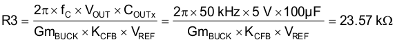
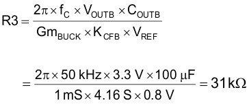
9.2.2.19 Selection of Components for Type II Compensation
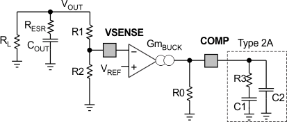 Figure 24. Buck Compensation Components
where
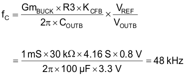
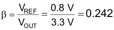
- VOUT = 5 V
- COUT = 100 µF
- GmBUCK = 1 mS
- VREF = 0.8 V
- KCFB = 0.125 / RSENSE = 8.33 S (0.125 is an internal constant)
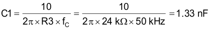
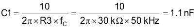
Use the standard value of R3 = 24 kΩ.
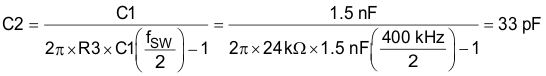
Use the standard value of 1.5 nF.
The resulting bandwidth of buck converter, f C, is calculated with Equation 28.
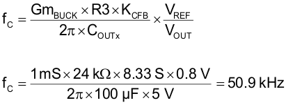
fC is close to the target bandwidth of 50 kHz.
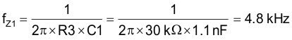
The resulting zero frequency, fZ1, is calculated with Equation 29.
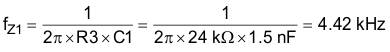
fZ1 is close to the fC / 10 guideline of 5 kHz.
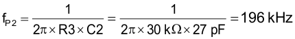
The second pole frequency, fP2, is calculated with Equation 30.
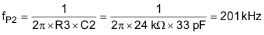
fP2 is close to the fSW / 2 guideline of 200 kHz. Hence, the design satisfies all requirements for a good loop.
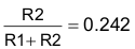
9.2.2.20 Resistor Divider Selection for Setting VOUTA Voltage
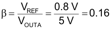
Select the divider current through R1 and R2 to be 50 µA. Then use Equation 32 and Equation 33 to find the values of R1 and R2.
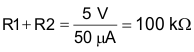
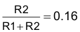
Therefore, R2 = 16 kΩ and R1 = 84 kΩ.
9.2.2.21 BuckB Component Selection
Using the same method as for VBuckA produces the following parameters and components.
This value is higher than the minimum duty cycle specified (100 ns typical).
∆Iripple current ≈ 0.4 A (approximately 20% of IOUT max)
Select an output capacitance COUTB of 100 µF with low ESR in the range of 10 mΩ.
Assume fC = 50 kHz.


Use the standard value of R3 = 30 kΩ.

fC is close to the target bandwidth of 50 kHz.
The resulting zero frequency, fZ1, is calculated with Equation 43.
fZ1 is close to the fC guideline of 5 kHz.
The second pole frequency, fP2, is calculated with Equation 44.
fP2 is close to the fSW / 2 guideline of 200 kHz.
Therefore the design satisfies all requirements for a good loop.
9.2.2.22 Resistor Divider Selection for Setting VOUT Voltage
Select the divider current through R1 and R2 to be 50 µA. Then use Equation 46 and Equation 47 to calculate the values of R1 and R2.

Therefore, R2 = 16 kΩ and R1 = 50 kΩ.
9.2.2.23 BuckX High-Side and Low-Side N-Channel MOSFETs
An internal supply, which is 5.8 V typical under normal operating conditions, provides the gate-drive supply for these MOSFETs. The output is a totem pole, allowing full-voltage drive of VREG to the gate with peak output current of 1.5 A. The reference for the high-side MOSFET is a floating node at the phase terminal (PHx), and the reference for the low-side MOSFET is the power-ground (PGNDx) terminal. For a particular application, select these MOSFETs with consideration for the following parameters: rDS(on), gate charge Qg, drain-to-source breakdown voltage BVDSS, maximum dc current IDC(max), and thermal resistance for the package.
The times tr and tf denote the rising and falling times of the switching node and have a relationship to the gate-driver strength of the TPS4333x-Q1 family of devices and to the gate Miller capacitance of the MOSFET. The first term denotes the conduction losses, which are minimal when the on-resistance of the MOSFET is low. The second term denotes the transition losses, which arise because of the full application of the input voltage across the drain-source of the MOSFET as it turns on or off. Transition losses are lower at low currents and when the switching time is low.

In addition, during the dead time td when both the MOSFETs are off, the body diode of the low-side MOSFET conducts, increasing the losses. The second term in the preceding equation denotes this. Using external Schottky diodes in parallel with the low-side MOSFETs of the buck converters helps to reduce this loss.
NOTE
The value of rDS(on) has a positive temperature coefficient, and the TC term for rDS(on) accounts for that fact. TC = d × ΔT(°C). The temperature coefficient d is available as a normalized value from MOSFET data sheets and can have an assumed starting value of 0.005 per ºC.
9.2.3 Application Curves
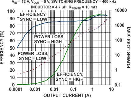 Figure 25. Efficiency Across Output Currents (Bucks)
 Figure 26. Efficiency Across Output Currents (Boost)