SLVSA82F March 2011 – December 2014 TPS43330-Q1 , TPS43332-Q1
PRODUCTION DATA.
- 1 Features
- 2 Applications
- 3 Description
- 4 Revision History
- 5 Device Comparison Table
- 6 Pin Configuration and Functions
- 7 Specifications
-
8 Detailed Description
- 8.1 Overview
- 8.2 Functional Block Diagram
- 8.3 Feature Description
- 8.4 Device Functional Modes
-
9 Application and Implementation
- 9.1 Application Information
- 9.2
Typical Application
- 9.2.1 Design Requirements
- 9.2.2
Detailed Design Procedure
- 9.2.2.1 Boost Component Selection
- 9.2.2.2 Boost Maximum Input Current IIN_MAX
- 9.2.2.3 Boost Inductor Selection, L
- 9.2.2.4 Inductor Ripple Current, IRIPPLE
- 9.2.2.5 Peak Current in Low-Side FET, IPEAK
- 9.2.2.6 Right Half-Plane Zero RHP Frequency, fRHP
- 9.2.2.7 Output Capacitor, COUTx
- 9.2.2.8 Bandwidth of Boost Converter, fC
- 9.2.2.9 Output Ripple Voltage Due to Load Transients, ∆VOUTx
- 9.2.2.10 Selection of Components for Type II Compensation
- 9.2.2.11 Input Capacitor, CIN
- 9.2.2.12 Output Schottky Diode D1 Selection
- 9.2.2.13 Low-Side MOSFET (BOT_SW3)
- 9.2.2.14 BuckA Component Selection
- 9.2.2.15 Inductor Selection L
- 9.2.2.16 Inductor Ripple Current IRIPPLE
- 9.2.2.17 Output Capacitor COUTA
- 9.2.2.18 Bandwidth of Buck Converter fC
- 9.2.2.19 Selection of Components for Type II Compensation
- 9.2.2.20 Resistor Divider Selection for Setting VOUTA Voltage
- 9.2.2.21 BuckB Component Selection
- 9.2.2.22 Resistor Divider Selection for Setting VOUT Voltage
- 9.2.2.23 BuckX High-Side and Low-Side N-Channel MOSFETs
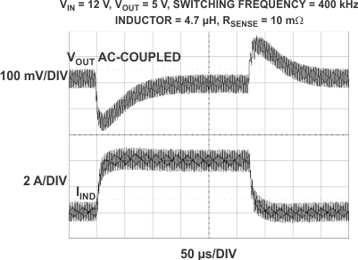
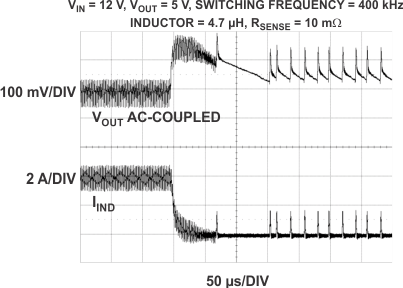
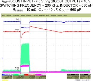
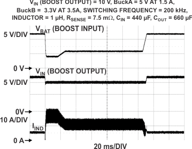
- 9.2.3 Application Curves
- 10Power Supply Recommendations
- 11Layout
- 12Device and Documentation Support
- 13Mechanical, Packaging, and Orderable Information
Package Options
Mechanical Data (Package|Pins)
- DAP|38
Thermal pad, mechanical data (Package|Pins)
- DAP|38
Orderable Information
7 Specifications
7.1 Absolute Maximum Ratings(1)
(1) Stresses beyond those listed under Absolute Maximum Ratings may cause permanent damage to the device. These are stress ratings only, and functional operation of the device at these or any other conditions beyond those indicated under Recommended Operating Conditions is not implied. Exposure to absolute-maximum-rated conditions for extended periods may affect device reliability. All voltage values are with respect to AGND, unless otherwise specified.
7.2 ESD Ratings
| VALUE | UNIT | |||||
|---|---|---|---|---|---|---|
| V(ESD) | Electrostatic discharge | Human body model (HBM), per AEC Q100-002(1) | ±2000 | V | ||
| Charged device model (CDM), per AEC Q100-011 | Corner pins: VBAT (1), ENC (19), SYNC (20), VIN (38) | ±750 | ||||
| Other pins | ±500 | |||||
(1) AEC Q100-002 indicates HBM stressing is done in accordance with the ANSI/ESDA/JEDEC JS-001 specification.
7.3 Recommended Operating Conditions
| MIN | NOM | MAX | UNIT | ||
|---|---|---|---|---|---|
| Buck function: BuckA and BuckB voltage |
Input voltage: VIN, VBAT | 4 | 40 | V | |
| Enable inputs: ENA, ENB | 0 | 40 | |||
| Boot inputs: CBA, CBB | 4 | 48 | |||
| Phase inputs: PHA, PHB | –0.6 | 40 | |||
| Current-sense voltage: SA1, SA2, SB1, SB2 | 0 | 11 | |||
| Power-good output: PGA, PGB | 0 | 11 | |||
| SYNC, EXTSUP | 0 | 9 | |||
| Boost function | Enable input: ENC | 0 | 9 | V | |
| Voltage sense: DS | 40 | ||||
| DIV | 0 | VREG | |||
| Operating temperature: TA | –40 | 125 | °C |
7.4 Thermal Information
| THERMAL METRIC(1) | TPS4333x-Q1 | UNIT | |
|---|---|---|---|
| DAP | |||
| 38 PINS | |||
| RθJA | Junction-to-ambient thermal resistance(2) | 27.3 | °C/W |
| RθJC(top) | Junction-to-case (top) thermal resistance(3) | 19.6 | |
| RθJB | Junction-to-board thermal resistance(4) | 15.9 | |
| ψJT | Junction-to-top characterization parameter(5) | 0.24 | |
| ψJB | Junction-to-board characterization parameter(6) | 6.6 | |
| RθJC(bot) | Junction-to-case (bottom) thermal resistance(7) | 1.2 | |
(1) For more information about traditional and new thermal metrics, see the IC Package Thermal Metrics application report, SPRA953.
(2) The junction-to-ambient thermal resistance under natural convection is obtained in a simulation on a JEDEC-standard, high-K board, as specified in JESD51-7, in an environment described in JESD51-2a.
(3) The junction-to-case (top) thermal resistance is obtained by simulating a cold plate test on the package top. No specific JEDEC-standard test exists, but a close description can be found in the ANSI SEMI standard G30-88.
(4) The junction-to-board thermal resistance is obtained by simulating in an environment with a ring cold plate fixture to control the PCB temperature, as described in JESD51-8.
(5) The junction-to-top characterization parameter, ψJT, estimates the junction temperature of a device in a real system and is extracted from the simulation data for obtaining RθJA, using a procedure described in JESD51-2a (sections 6 and 7).
(6) The junction-to-board characterization parameter, ψJB, estimates the junction temperature of a device in a real system and is extracted from the simulation data for obtaining RθJA, using a procedure described in JESD51-2a (sections 6 and 7).
(7) The junction-to-case (bottom) thermal resistance is obtained by simulating a cold plate test on the exposed (power) pad. No specific JEDEC standard test exists, but a close description can be found in the ANSI SEMI standard G30-88.
7.5 Electrical Characteristics
VIN = 8 V to 18 V, TJ = –40°C to 150°C (unless otherwise noted)| NO. | PARAMETER | TEST CONDITIONS | MIN | TYP | MAX | UNIT | |
|---|---|---|---|---|---|---|---|
| 1.0 | INPUT SUPPLY | ||||||
| 1.1 | VBAT | Supply voltage | Boost controller enabled, after satisfying initial start-up condition | 2 | 40 | V | |
| 1.2 | VIN | Input voltage required for device on initial start-up | 6.5 | 40 | V | ||
| Buck regulator operating range after initial start-up | 4 | 40 | |||||
| 1.3 | VIN(UV) | Buck undervoltage lockout | VIN falling. After a reset, initial start-up conditions may apply.(3) | 3.5 | 3.6 | 3.8 | V |
| VIN rising. After a reset, initial start-up conditions may apply.(3) | 3.8 | 4 | V | ||||
| 1.4 | VBOOST_UNLOCK | Boost unlock threshold | VBAT rising | 8.2 | 8.5 | 8.8 | V |
| 1.5 | Iq_LPM_ | LPM quiescent current: (1) |
VIN = 13 V, BuckA: LPM, BuckB: off, TA = 25°C | 30 | 40 | µA | |
| VIN = 13 V, BuckB: LPM, BuckA: off, TA = 25°C | |||||||
| VIN = 13 V, BuckA, B: LPM, TA = 25°C | 35 | 45 | µA | ||||
| 1.6 | Iq_LPM | LPM quiescent current: (1) |
VIN = 13 V, BuckA: LPM, BuckB: off, TA = 125°C | 40 | 50 | µA | |
| VIN = 13 V, BuckB: LPM, BuckA: off, TA = 125°C | |||||||
| VIN = 13 V, BuckA, B: LPM, TA = 125°C | 45 | 55 | µA | ||||
| 1.7 | Iq_NRM | Quiescent current: normal (PWM) mode(1) |
SYNC = HIGH, TA = 25°C | 4.85 | 5.3 | mA | |
| VIN = 13 V, BuckA: CCM, BuckB: off, TA = 25°C | |||||||
| VIN = 13 V, BuckB: CCM, BuckA: off, TA = 25°C | |||||||
| VIN = 13 V, BuckA, B: CCM, TA = 25°C | 7 | 7.6 | |||||
| 1.8 | Iq_NRM | Quiescent current: normal (PWM) mode(1) |
SYNC = HIGH, TA = 125°C | 5 | 5.5 | mA | |
| VIN = 13 V, BuckA: CCM, BuckB: off, TA = 125°C | |||||||
| VIN = 13 V, BuckB: CCM, BuckA: off, TA = 125°C | |||||||
| VIN = 13 V, BuckA, B: CCM, TA = 125°C | 7.5 | 8 | |||||
| 1.9 | Ibat_sh | Shutdown current | BuckA, B: off, VBAT = 13 V , TA = 25°C | 2.5 | 4 | µA | |
| 1.10 | Ibat_sh | Shutdown current | BuckA, B: off, VBAT = 13 V, TA = 125°C | 3 | 5 | µA | |
| 2.0 | INPUT VOLTAGE VBAT — UNDERVOLTAGE LOCKOUT | ||||||
| 2.1 | VBAT(UV) | Boost-input undervoltage | VBAT falling. After a reset, initial start-up conditions may apply.(3) | 1.8 | 1.9 | 2 | V |
| VBAT rising. After a reset, initial start-up conditions may apply.(3) | 2.4 | 2.5 | 2.6 | V | |||
| 2.2 | UVLOHys | Hysteresis | 500 | 600 | 700 | mV | |
| 2.3 | UVLOfilter | Filter time | 5 | µs | |||
| 3.0 | INPUT VOLTAGE VIN — OVERVOLTAGE LOCKOUT | ||||||
| 3.1 | VOVLO | Overvoltage shutdown | VIN rising | 45 | 46 | 47 | V |
| VIN falling | 43 | 44 | 45 | ||||
| 3.2 | OVLOHys | Hysteresis | 1 | 2 | 3 | V | |
| 3.3 | OVLOfilter | Filter time | 5 | µs | |||
| 4.0 | BOOST CONTROLLER | ||||||
| 4.1 | Vboost7V | Boost VOUT = 7 V | DIV = low, VBAT = 2 V to 7 V | 6.8 | 7 | 7.3 | V |
| 4.2 | Vboost7V-th | Boost-enable threshold | Boost VOUT = 7 V, VBAT falling | 7.5 | 8 | 8.5 | V |
| Boost-disable threshold | Boost VOUT = 7 V, VBAT rising | 8 | 8.5 | 9 | |||
| Boost hysteresis | Boost VOUT = 7 V, VBAT rising or falling | 0.4 | 0.5 | 0.6 | |||
| 4.3 | Vboost10V | Boost VOUT = 10 V | DIV = open, VBAT = 2 V to 10 V | 9.7 | 10 | 10.4 | V |
| 4.4 | Vboost10V-th | Boost-enable threshold | Boost VOUT = 10 V, VBAT falling | 10.5 | 11 | 11.5 | V |
| Boost-disable threshold | Boost VOUT = 10 V, VBAT rising | 11 | 11.5 | 12 | |||
| Boost hysteresis | Boost VOUT = 10 V, VBAT rising or falling | 0.4 | 0.5 | 0.6 | |||
| 4.5 | Vboost11V | Boost VOUT = 11 V | DIV = VREG, VBAT = 2 V to 11 V | 10.7 | 11 | 11.4 | V |
| 4.6 | Vboost11V-th | Boost-enable threshold | Boost VOUT = 11 V, VBAT falling | 11.5 | 12 | 12.5 | V |
| Boost-disable threshold | Boost VOUT = 11 V, VBAT rising | 12 | 12.5 | 13 | |||
| Boost hysteresis | Boost VOUT = 11 V, VBAT rising or falling | 0.4 | 0.5 | 0.6 | |||
| BOOST-SWITCH CURRENT LIMIT | |||||||
| 4.7 | VDS | Current-limit sensing | DS input with respect to PGNDA | 0.175 | 0.2 | 0.225 | V |
| 4.8 | tDS | Leading-edge blanking | 200 | ns | |||
| GATE DRIVER FOR BOOST CONTROLLER | |||||||
| 4.9 | IGC1 Peak | Gate-driver peak current | 1.5 | A | |||
| 4.10 | rDS(on) | Source and sink driver | VREG = 5.8 V, IGC1 current = 200 mA | 2 | Ω | ||
| GATE DRIVER FOR PMOS | |||||||
| 4.11 | rDS(on) | PMOS OFF | 10 | 20 | Ω | ||
| 4.12 | IPMOS_ON | Gate current | VIN = 13.5 V, VGS = –5 V | 10 | mA | ||
| 4.13 | tdelay_ON | Turnon delay | C = 10 nF | 5 | 10 | µs | |
| BOOST-CONTROLLER SWITCHING FREQUENCY | |||||||
| 4.14 | fsw-Boost | Boost switching frequency | fSW_Buck / 2 | kHz | |||
| 4.15 | DBoost | Boost duty cycle | 90% | ||||
| ERROR AMPLIFIER (OTA) FOR BOOST CONVERTERS | |||||||
| 4.16 | GmBOOST | Forward transconductance | VBAT = 12 V | 0.8 | 1.35 | mS | |
| VBAT = 5 V | 0.35 | 0.65 | |||||
| 5.0 | BUCK CONTROLLERS | ||||||
| 5.1 | VBuckA or VBuckB | Adjustable output-voltage range | 0.9 | 11 | V | ||
| 5.2 | Vref, NRM | Internal reference and tolerance voltage in normal mode | Measure FBX pin | 0.792 | 0.8 | 0.808 | V |
| –1% | 1% | ||||||
| 5.3 | Vref, LPM | Internal reference and tolerance voltage in low-power mode | Measure FBX pin | 0.784 | 0.8 | 0.816 | V |
| –2% | 2% | ||||||
| 5.4 | Vsense | V sense for forward-current limit in CCM | FBx = 0.75 V (low duty cycle) | 60 | 75 | 90 | mV |
| 5.5 | V sense for reverse-current limit in CCM | FBx = 1 V | –65 | –37.5 | –23 | mV | |
| 5.6 | VI-Foldback | V sense for output short | FBx = 0 V | 17 | 32.5 | 48 | mV |
| 5.7 | tdead | Shoot-through delay, blanking time | 20 | ns | |||
| 5.8 | DCNRM | High-side minimum on-time | 100 | ns | |||
| Maximum duty cycle (digitally controlled) | 98.75% | ||||||
| 5.9 | DCLPM | Duty cycle, LPM | 80% | ||||
| 5.10 | ILPM_Entry | LPM entry-threshold load current as fraction of maximum set load current | 1% | See (2) | |||
| ILPM_Exit | LPM exit-threshold load current as fraction of maximum set load current | See (2) | 10% | ||||
| HIGH-SIDE EXTERNAL NMOS GATE DRIVERS FOR BUCK CONTROLLER | |||||||
| 5.11 | IGX1_peak | Gate-driver peak current | 1.5 | A | |||
| 5.12 | rDS(on) | Source and sink driver | VREG = 5.8 V, IGX1 current = 200 mA | 2 | Ω | ||
| LOW-SIDE NMOS GATE DRIVERS FOR BUCK CONTROLLER | |||||||
| 5.13 | IGX2_peak | Gate-driver peak current | 1.5 | A | |||
| 5.14 | RDS ON | Source and sink driver | VREG = 5.8 V, IGX2 current = 200 mA | 2 | Ω | ||
| ERROR AMPLIFIER (OTA) FOR BUCK CONVERTERS | |||||||
| 5.15 | GmBUCK | Transconductance | COMPA, COMPB = 0.8 V, source/sink = 5 µA, test in feedback loop |
0.72 | 1 | 1.35 | mS |
| 5.16 | IPULLUP_FBx | Pullup current at FBx pins | FBx = 0 V | 50 | 100 | 200 | nA |
| 6.0 | DIGITAL INPUTS: ENA, ENB, ENC, SYNC | ||||||
| 6.1 | VIH | Higher threshold | VIN = 13 V | 1.7 | V | ||
| 6.2 | VIL | Lower threshold | VIN = 13 V | 0.7 | V | ||
| 6.3 | RIH_SYNC | Pulldown resistance on SYNC | VSYNC = 5 V | 500 | kΩ | ||
| 6.4 | RIL_ENC | Pulldown resistance on ENC | VENC = 5 V | 500 | kΩ | ||
| 6.5 | IIL_ENx | Pullup current source on ENA, ENB | VENx = 0 V | 0.5 | 2 | µA | |
| 7.0 | BOOST OUTPUT VOLTAGE: DIV | ||||||
| 7.1 | VIH_DIV | Higher threshold | VREG = 5.8 V | VREG – 0.2 | V | ||
| 7.2 | VIL_DIV | Lower threshold | 0.2 | V | |||
| 7.3 | Voz_DIV | Voltage on DIV if unconnected | Voltage on DIV if unconnected | VREG / 2 | V | ||
| 8.0 | SWITCHING PARAMETER – BUCK DC-DC CONTROLLERS | ||||||
| 8.1 | fSW_Buck | Buck switching frequency | RT pin: GND | 360 | 400 | 440 | kHz |
| 8.2 | fSW_Buck | Buck switching frequency | RT pin: 60-kΩ external resistor | 360 | 400 | 440 | kHz |
| 8.3 | fSW_adj | Buck adjustable range with external resistor | RT pin: external resistor | 150 | 600 | kHz | |
| 8.4 | fSYNC | Buck synchronization range | External clock input | 150 | 600 | kHz | |
| 8.5 | fSS | Spread-spectrum spreading | TPS43332-Q1 only | 5% | |||
| 9.0 | INTERNAL GATE-DRIVER SUPPLY | ||||||
| 9.1 | VREG | Internal regulated supply | VIN = 8 V to 18 V, VEXTSUP = 0 V, SYNC = high | 5.5 | 5.8 | 6.1 | V |
| Load regulation | IVREG = 0 mA to 100 mA, VEXTSUP = 0 V, SYNC = high |
0.2% | 1% | ||||
| 9.2 | VREG(EXTSUP) | Internal regulated supply | VEXTSUP = 8.5 V | 7.2 | 7.5 | 7.8 | V |
| Load regulation | IEXTSUP = 0 mA to 125 mA, SYNC = High VEXTSUP = 8.5 V to 13 V |
0.2% | 1% | ||||
| 9.3 | VEXTSUP-th | EXTSUP switch-over voltage threshold | IVREG = 0 mA to 100 mA, VEXTSUP ramping positive |
4.4 | 4.6 | 4.8 | V |
| 9.4 | VEXTSUP-Hys | EXTSUP switch-over hysteresis | 150 | 250 | mV | ||
| 9.5 | IVREG-Limit | Current limit on VREG | VEXTSUP = 0 V, normal mode as well as LPM | 100 | 400 | mA | |
| 9.6 | IVREG_EXTSUP-Limit | Current limit on VREG when using EXTSUP | IVREG = 0 mA to 100 mA, VEXTSUP = 8.5 V, SYNC = High |
125 | 400 | mA | |
| 10.0 | SOFT START | ||||||
| 10.1 | ISSx | Soft-start source current | VSSA and VSSB = 0 V | 0.75 | 1 | 1.25 | µA |
| 11.0 | OSCILLATOR (RT) | ||||||
| 11.1 | VRT | Oscillator reference voltage | 1.2 | V | |||
| 12.0 | POWER GOOD / DELAY | ||||||
| 12.1 | PGpullup | Pullup for A and B to Sx2 | 50 | kΩ | |||
| 12.2 | PGth1 | Power-good threshold | FBx falling | –5% | –7% | –9% | |
| 12.3 | PGhys | Hysteresis | 2% | ||||
| 12.4 | PGdrop | Voltage drop | IPGA = 5 mA | 450 | mV | ||
| 12.5 | IPGA = 1 mA | 100 | mV | ||||
| 12.6 | PGleak | Power-good leakage | VSx2 = VPGx = 13 V | 1 | µA | ||
| 12.7 | tdeglitch | Power-good deglitch time | 2 | 16 | µs | ||
| 12.8 | tdelay | Reset delay | External capacitor = 1 nF VBuckX < PGth1 |
1 | ms | ||
| 12.9 | tdelay_fix | Fixed reset delay | No external capacitor, pin open | 20 | 50 | µs | |
| 12.10 | IOH | Activate current source (current to charge external capacitor) | 30 | 40 | 50 | µA | |
| 12.11 | IIL | Activate current sink (current to discharge external capacitor) | 30 | 40 | 50 | µA | |
| 13.0 | OVERTEMPERATURE PROTECTION | ||||||
| 13.1 | Tshutdown | Junction-temperature shutdown threshold | 150 | 165 | °C | ||
| 13.2 | Thys | Junction-temperature hysteresis | 15 | °C | |||
(1) Quiescent current specification is non-switching current consumption without including the current in the external-feedback resistor divider.
(2) The exit threshold specification is to be always higher than the entry threshold.
(3) If VBAT and VREG remain adequate, the buck can continue to operate if VIN is > 3.8 V.
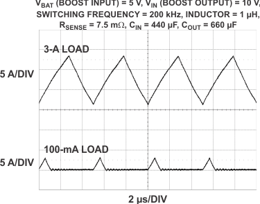
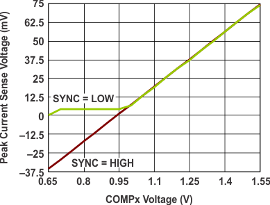
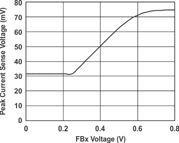
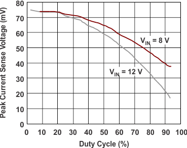
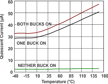
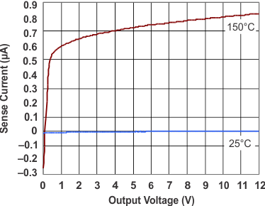
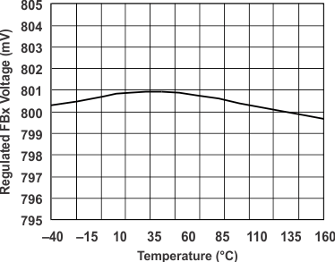
7.6 Typical Characteristics