SLVSBF0C JULY 2012 – April 2019 TPS53015
PRODUCTION DATA.
- 1 Features
- 2 Applications
- 3 Description
- 4 Revision History
- 5 Pin Configuration and Functions
- 6 Specifications
- 7 Detailed Description
- 8 Application and Implementation
- 9 Power Supply Recommendations
- 10Layout
- 11Device and Documentation Support
- 12Mechanical, Packaging, and Orderable Information
Package Options
Mechanical Data (Package|Pins)
- DGS|10
Thermal pad, mechanical data (Package|Pins)
Orderable Information
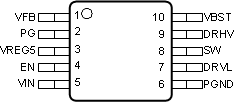
5 Pin Configuration and Functions
DGS Package
10-Pin VSSOP
Top View

Pin Functions
| PIN | I/O(1) | DESCRIPTION | |
|---|---|---|---|
| NAME | NO. | ||
| DRVH | 9 | O | High-side N-channel MOSFET gate driver output. SW referenced driver switches between SW(OFF) and VBST(ON). |
| DRVL | 7 | O | Low-side N-Channel MOSFET gate driver output. PGND referenced driver switches between PGND(OFF) and VREG5(ON). |
| EN | 4 | I | Enable. Pull high to enable converter. |
| PG | 2 | O | Open drain power good output. |
| PGND | 6 | I | System ground. |
| SW | 8 | I/O | Switch node connections for both the high-side driver and overcurrent comparator. |
| VBST | 10 | I | High-side MOSFET gate driver bootstrap voltage input. Connect a capacitor from VBST to SW. An internal diode is connected between VREG5 and VBST |
| VFB | 1 | I | D-CAP2 feedback input. Connect to output voltage with resistor divider. |
| VIN | 5 | I | Supply Input for 5-V linear regulator. Bypass to GND with a minimum 0.1-μF high quality ceramic capacitor. |
| VREG5 | 3 | O | Output of 5-V linear regulator and supply for MOSFET driver. Bypass to GND with a minimum 4.7-μF high-quality ceramic capacitor. VREG5 is active when EN is asserted high. |
(1) I = input, O = output