SLUSAE6B December 2010 – November 2023 TPS53315
PRODUCTION DATA
- 1
- 1 Features
- 2 Applications
- 3 Description
- 4 Pin Configuration and Functions
- 5 Specifications
-
6 Detailed Description
- 6.1 Overview
- 6.2 Functional Block Diagram
- 6.3
Feature Description
- 6.3.1 D-CAP™ Integrated Circuit with Adaptive On-Time
- 6.3.2 Small Signal Model
- 6.3.3 Ramp Signal
- 6.3.4 Auto-Skip Eco-mode Light Load Operation
- 6.3.5 Adaptive Zero Crossing
- 6.3.6 Forced Continuous Conduction Mode
- 6.3.7 Power Good
- 6.3.8 Current Sense and Overcurrent Protection
- 6.3.9 Overvoltage and Undervoltage Protection
- 6.3.10 UVLO Protection
- 6.3.11 Thermal Shutdown
- 6.4 Device Functional Modes
-
7 Application and Implementation
- 7.1 Application Information
- 7.2
Typical Application
- 7.2.1
Typical Application Circuit Diagram
- 7.2.1.1 Design Requirements
- 7.2.1.2
Detailed Design Procedure
- 7.2.1.2.1 Step 1: Select Operation Mode and Soft-Start Time
- 7.2.1.2.2 Step 2: Select Switching Frequency
- 7.2.1.2.3 Step 3: Select the Inductance
- 7.2.1.2.4 Step 4: Select Output Capacitors
- 7.2.1.2.5 Step 5: Determine the Voltage-Divider Resistance (R1 and R2)
- 7.2.1.2.6 Step 6: Select the Overcurrent Resistance (RTRIP)
- 7.2.1.3 Application Curves
- 7.2.2 Typical Application Circuit Diagram With Ceramic Output Capacitors
- 7.2.1
Typical Application Circuit Diagram
- 7.3 Power Supply Recommendations
- 7.4 Layout
- 8 Device and Documentation Support
- 9 Revision History
- 10Mechanical, Packaging, and Orderable Information
Package Options
Mechanical Data (Package|Pins)
- RGF|40
Thermal pad, mechanical data (Package|Pins)
- RGF|40
Orderable Information
6.3.4 Auto-Skip Eco-mode Light Load Operation
While the MODE pin is pulled low through RMODE, the TPS53315 automatically reduces the switching frequency at light-load conditions to maintain high efficiency. Detailed operation is described as follows. As the output current decreases from heavy load condition, the inductor current is also reduced and eventually comes to the point that its rippled valley touches zero level, which is the boundary between continuous conduction and discontinuous conduction modes. The synchronous MOSFET is turned off when this zero inductor current is detected. As the load current further decreases, the converter runs into discontinuous conduction mode (DCM). The on-time is maintained as it was in the continuous conduction mode so that it takes longer time to discharge the output capacitor with smaller load current to the level of the reference voltage. The transition point to the light-load operation IOUT(LL) (that is, the threshold between continuous and discontinuous conduction mode) can be calculated as shown in Equation 3.
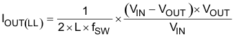
where
- ƒSW is the PWM switching frequency
Switching frequency versus output current in the light load condition is a function of L, VIN and VOUT, but it decreases almost proportionally to the output current from the IOUT(LL) given in Equation 3. For example, it is 60 kHz at IOUT(LL)/5 if the frequency setting is 300 kHz.