SLUSC63A November 2015 – December 2015 TPS53317A
PRODUCTION DATA.
- 1 Features
- 2 Applications
- 3 Description
- 4 Revision History
- 5 Pin Configuration and Functions
- 6 Specifications
- 7 Detailed Description
- 8 Application and Implementation
- 9 Power Supply Recommendations
- 10Layout
- 11Device and Documentation Support
- 12Mechanical, Packaging, and Orderable Information
Package Options
Mechanical Data (Package|Pins)
- RGB|20
Thermal pad, mechanical data (Package|Pins)
- RGB|20
Orderable Information
8 Application and Implementation
NOTE
Information in the following applications sections is not part of the TI component specification, and TI does not warrant its accuracy or completeness. TI’s customers are responsible for determining suitability of components for their purposes. Customers should validate and test their design implementation to confirm system functionality.
8.1 Application Information
The TPS53317A device is a FET-integrated synchronous buck regulator designed mainly for DDR termination. It can provide a regulated output at ½ VDDQ with both sink and source capability. The device employs D-CAP+ mode operation that provides ease-of-use, low external component count and fast transient response.
8.2 Typical Applications
8.2.1 DDR4 SDRAM Application
This DDR4 application requires a tight load tolerance, fast transient response, and sinking current capability, the design uses a non-droop PWM configuration.
8.2.1.1 Design Requirements
- Input voltage : VIN = 1.2 V
- Output voltage: VOUT = 0.6 V
- Maximum load step size of 3 A @ slew rate 7 A/µs (–1.5 A to 1.5 A)
- DC +AC + Ripple voltage regulation limit at sense point: ±42 mV (0.642 V overshoot, 0.558 V undershoot)
- Maximum load: IMAX = 2.5 A
8.2.1.2 Detailed Design Procedure
8.2.1.2.1 Step 1. Determine Configuration
Because this DDR4 application requires a tight load tolerance, fast transient response, and sinking current capability, the design uses a non-droop PWM configuration. Choose 600-kHz switching frequency due to the duty cycle and minimim off-time of the device, and set an overcurrent (OC) valley limit of 5.4 A due to the maximum load requirement of 2.5 A. Referring to Table 1 select an RMODE value of 68 kΩ.
8.2.1.2.2 Step 2. Select Inductor
Smaller inductor values have better transient performance but higher ripple and lower efficiency. High values have the opposite characteristics. It is common practice to limit the ripple current to 30% to 50% of the maximum current. Choose 50% to allow use of a smaller inductor for faster transient performance.


where
- D = duty cycle
Because this device operates in DCAP+ mode, the frequency and duty cycle vary based on the input voltage, the output voltage and load. With a 2.5-A load, a 1.2-V input voltage and 0.60 V output voltage, fSW is experimentally measured at approximately 800 kHz and duty cycle of 0.55. Therefore L is calculated as shown in Equation 10.

Choose the closest standard value, 0.25 µH.
8.2.1.2.3 Step 3. Determine Output Capacitance
Use Equation 10 to calculate the output capacitance for a desired maximum overshoot.

where
- COUT(min),OS is the minimum output capacitance for a desired overshoot
- ΔIOUT is the maximum output current change in the application
- VOUT = desired output voltage
- VOS is the desired output voltage change due to overshoot
Choose a value of 30 mV to account for normal output voltage ripple.

Use Equation 12 to calculate the necessary output capacitance for a desired maximum undershoot.

where
- COUT(min),US is the minimum output capacitance for a desired undershoot
- VUS is the desired output voltage change due to overshoot
- tSW is the period of switch node
- tMIN(off) is the minimum off-time (270 ns)
Again, choose 30 mV to account for normal output voltage ripple.

The undershoot requirements determine, so there must be a minimum of 157.6 µF. Because this is a DDR application where size is also a consideration, this design uses only ceramic capacitors. To account for voltage de-rating of capacitors and provide additional margin, this design includes eleven 22-µF output capacitors.
8.2.1.2.4 Step 4. Input Capacitance
This design requires sufficient input capacitance to filter the input current from the host source. Use Equation 14 to calculate the necessary input capacitance.

where
- ΔVIN(P-P) is the desired input voltage ripple (typically 1% of the input voltage)

As with the output capacitance selection, this design accounts for voltage de-rating of capacitors and provides additional margin, using four 22-µF input capacitors.
8.2.1.2.5 Step 5. Compensation Network
In order to achieve stable operation, the crossover frequency should be less than 1/5 of the switching frequency.

where
- RS = 53 mΩ
Account for capacitor de-rating here and set the value of COUT to 160 µF, so that Equation 17 is true.

Choose an RC value of 3.9 kΩ. Determine CC by choosing the value of the zero created by RC and CC. Using the relationship described in Equation 18.

Equation 18 yields a CC value of 2.55 nF. Choose the closest common capacitor value of 2.2 nF. To determine a value for CP, first consider the relationship described in Equation 19.

where
- CC >> CP
Because CC >> CP , set the pole to be two times the switching frequency as described in Equation 20.

To boost the gain margin, set CP to 33 pF.
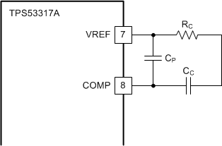 Figure 31. Compensation Network Circuit
8.2.1.2.6 Peripheral Component Selection
As described in Table 1, connect a 0.22-µF capacitor from the VREF pin to GND and connect a 0.1-µF bootstrap capacitor from the SW pin to the BST pin. Because the PGOOD pin is open drain, connect a pullup resistor between it and the 5-V rail.
8.2.1.3 Application Curves
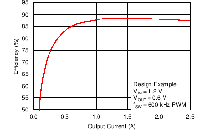
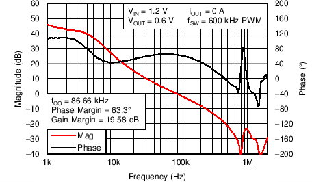 Figure 34. Bode Plot, No Load
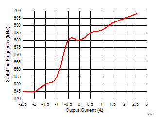
| VIN = 1.2 | fSW = 600 kHz |
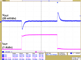 Figure 33. Load Transient
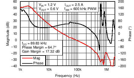 Figure 35. Bode Plot, Full Load
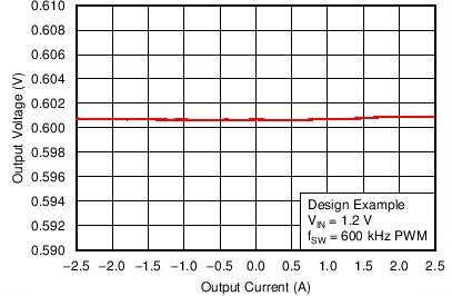
8.2.2 DDR3 SDRAM Application
8.2.2.1 Design Requirements
- VIN = 1.5 V
- VOUT = 0.75 V
8.2.3 Non-Tracking Point-of-Load (POL) Application
8.2.3.1 Design Requirements
- VIN = 3.3 V
- VOUT = 1.2 V
8.2.3.2 Application Curves
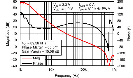 Figure 40. Bode Plot No Load
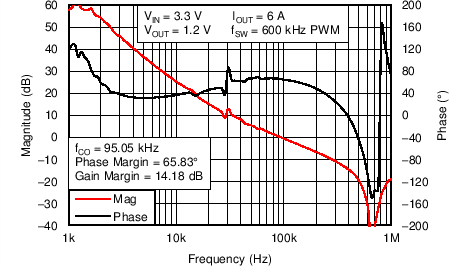 Figure 41. Bode Plot Full Load