SLVSCF8 July 2014 TPS54060-EP
PRODUCTION DATA.
- 1 Features
- 2 Applications
- 3 Description
- 4 Simplified Schematic
- 5 Revision History
- 6 Pin Configuration and Functions
- 7 Specifications
-
8 Detailed Description
- 8.1 Overview
- 8.2 Functional Block Diagram
- 8.3
Feature Description
- 8.3.1 Fixed Frequency PWM Control
- 8.3.2 Slope Compensation Output Current
- 8.3.3 Low-Dropout Operation and Bootstrap Voltage (Boot)
- 8.3.4 Error Amplifier
- 8.3.5 Voltage Reference
- 8.3.6 Adjusting the Output Voltage
- 8.3.7 Enable and Adjusting UVLO
- 8.3.8 Slow Start/Tracking Pin (SS/TR)
- 8.3.9 Overload Recovery Circuit
- 8.3.10 Sequencing
- 8.3.11 Constant Switching Frequency and Timing Resistor (RT/CLK Pin)
- 8.3.12 Overcurrent Protection and Frequency Shift
- 8.3.13 Selecting the Switching Frequency
- 8.3.14 How to Interface to RT/CLK Pin
- 8.3.15 Power Good (PWRGD Pin)
- 8.3.16 Overvoltage Transient Protection (OVTP)
- 8.3.17 Thermal Shutdown
- 8.3.18 Small Signal Model for Loop Response
- 8.3.19 Simple Small Signal Model for Peak Current Mode Control
- 8.3.20 Small Signal Model for Frequency Compensation
- 8.4 Device Functional Modes
-
9 Application and Implementation
- 9.1 Application Information
- 9.2
Typical Application
- 9.2.1 Design Requirements
- 9.2.2
Detailed Design Procedure
- 9.2.2.1 Selecting the Switching Frequency
- 9.2.2.2 Output Inductor Selection (LO)
- 9.2.2.3 Output Capacitor
- 9.2.2.4 Catch Diode
- 9.2.2.5 Input Capacitor
- 9.2.2.6 Slow Start Capacitor
- 9.2.2.7 Bootstrap Capacitor Selection
- 9.2.2.8 UVLO Set Point
- 9.2.2.9 Output Voltage and Feedback Resistors Selection
- 9.2.2.10 Compensation
- 9.2.3 Application Curves
- 10Power Supply Recommendations
- 11Layout
- 12Device and Documentation Support
- 13Mechanical, Packaging, and Orderable Information
Package Options
Mechanical Data (Package|Pins)
- DGQ|10
Thermal pad, mechanical data (Package|Pins)
- DGQ|10
Orderable Information
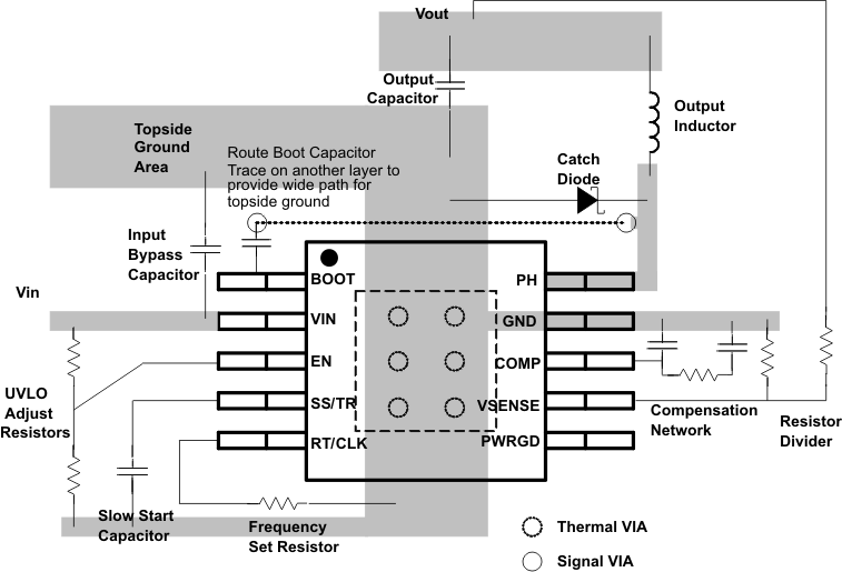
11 Layout
11.1 Layout Guidelines
Layout is a critical portion of good power supply design. There are several signals paths that conduct fast changing currents or voltages that can interact with stray inductance or parasitic capacitance to generate noise or degrade the power supplies performance. To help eliminate these problems, the VIN pin should be bypassed to ground with a low-ESR ceramic bypass capacitor with X5R or X7R dielectric. Take care to minimize the loop area formed by the bypass capacitor connections, the VIN pin, and the anode of the catch diode. See Layout Example for a PCB layout example. The GND pin should be tied directly to the power pad under the IC and the power pad.
The power pad should be connected to any internal PCB ground planes using multiple vias directly under the IC. The PH pin should be routed to the cathode of the catch diode and to the output inductor. Because the PH connection is the switching node, the catch diode and output inductor should be located close to the PH pins, and the area of the PCB conductor minimized to prevent excessive capacitive coupling. For operation at full rated load, the top side ground area must provide adequate heat dissipating area. The RT/CLK pin is sensitive to noise so the RT resistor should be located as close as possible to the IC and routed with minimal lengths of trace. The additional external components can be placed approximately as shown. It may be possible to obtain acceptable performance with alternate PCB layouts; however, this layout has been shown to produce good results and is meant as a guideline.
11.1.1 Estimated Circuit Area
The estimated printed circuit board area for the components used in the design of Figure 50 is 0.55 inch2. This area does not include test points or connectors.
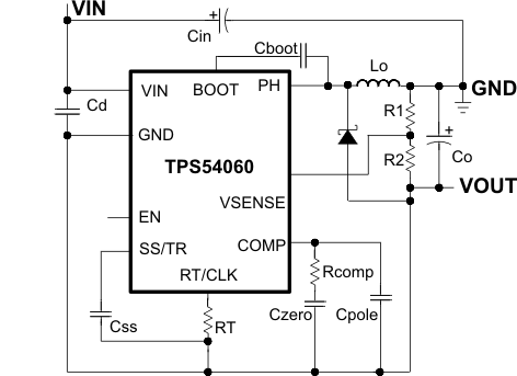 Figure 63. Inverting Power Supply from the SLVA317 Application Note
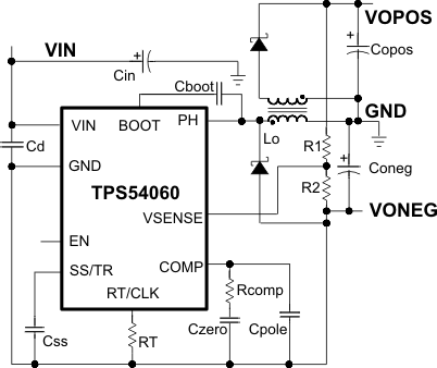 Figure 64. Split Rail Power Supply Based on the SLVA369 Application Note
11.2 Layout Example