SLVSCF8 July 2014 TPS54060-EP
PRODUCTION DATA.
- 1 Features
- 2 Applications
- 3 Description
- 4 Simplified Schematic
- 5 Revision History
- 6 Pin Configuration and Functions
- 7 Specifications
-
8 Detailed Description
- 8.1 Overview
- 8.2 Functional Block Diagram
- 8.3
Feature Description
- 8.3.1 Fixed Frequency PWM Control
- 8.3.2 Slope Compensation Output Current
- 8.3.3 Low-Dropout Operation and Bootstrap Voltage (Boot)
- 8.3.4 Error Amplifier
- 8.3.5 Voltage Reference
- 8.3.6 Adjusting the Output Voltage
- 8.3.7 Enable and Adjusting UVLO
- 8.3.8 Slow Start/Tracking Pin (SS/TR)
- 8.3.9 Overload Recovery Circuit
- 8.3.10 Sequencing
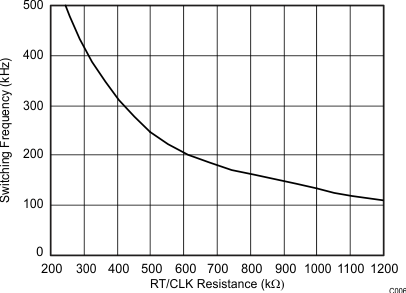
- 8.3.11 Constant Switching Frequency and Timing Resistor (RT/CLK Pin)
- 8.3.12 Overcurrent Protection and Frequency Shift
- 8.3.13 Selecting the Switching Frequency
- 8.3.14 How to Interface to RT/CLK Pin
- 8.3.15 Power Good (PWRGD Pin)
- 8.3.16 Overvoltage Transient Protection (OVTP)
- 8.3.17 Thermal Shutdown
- 8.3.18 Small Signal Model for Loop Response
- 8.3.19 Simple Small Signal Model for Peak Current Mode Control
- 8.3.20 Small Signal Model for Frequency Compensation
- 8.4 Device Functional Modes
-
9 Application and Implementation
- 9.1 Application Information
- 9.2
Typical Application
- 9.2.1 Design Requirements
- 9.2.2
Detailed Design Procedure
- 9.2.2.1 Selecting the Switching Frequency
- 9.2.2.2 Output Inductor Selection (LO)
- 9.2.2.3 Output Capacitor
- 9.2.2.4 Catch Diode
- 9.2.2.5 Input Capacitor
- 9.2.2.6 Slow Start Capacitor
- 9.2.2.7 Bootstrap Capacitor Selection
- 9.2.2.8 UVLO Set Point
- 9.2.2.9 Output Voltage and Feedback Resistors Selection
- 9.2.2.10 Compensation
- 9.2.3 Application Curves
- 10Power Supply Recommendations
- 11Layout
- 12Device and Documentation Support
- 13Mechanical, Packaging, and Orderable Information
Package Options
Mechanical Data (Package|Pins)
- DGQ|10
Thermal pad, mechanical data (Package|Pins)
- DGQ|10
Orderable Information
7 Specifications
7.1 Absolute Maximum Ratings(1)
over operating temperature range (unless otherwise noted)| MIN | MAX | UNIT | ||
|---|---|---|---|---|
| Input voltage | VIN | –0.3 | 65 | V |
| EN | –0.3 | 5 | ||
| BOOT | 75 | |||
| VSENSE | –0.3 | 3 | ||
| COMP | –0.3 | 3 | ||
| PWRGD | –0.3 | 6 | ||
| SS/TR | –0.3 | 3 | ||
| RT/CLK | –0.3 | 3.6 | ||
| Output voltage | BOOT-PH | 8 | V | |
| PH | –0.6 | 65 | ||
| PH, 10-ns transient | –2 | 65 | ||
| Voltage difference | PAD to GND | –200 | 200 | mV |
| Source current | EN | 100 | μA | |
| BOOT | 100 | mA | ||
| VSENSE | 10 | μA | ||
| PH | Current limit | A | ||
| RT/CLK | 100 | μA | ||
| Sink current | VIN | Current limit | A | |
| COMP | 100 | μA | ||
| PWRGD | 10 | mA | ||
| SS/TR | 200 | μA | ||
| Operating junction temperature | –55 | 150 | °C | |
(1) Stresses beyond those listed under Absolute Maximum Ratings may cause permanent damage to the device. These are stress ratings only and functional operation of the device at these or any other conditions beyond those indicated under Recommended Operating Conditions is not implied. Exposure to absolute-maximum-rated conditions for extended periods may affect device reliability.
7.2 Handling Ratings
| MIN | MAX | UNIT | |||
|---|---|---|---|---|---|
| Tstg | Storage temperature range | –65 | 150 | °C | |
| V(ESD) | Electrostatic discharge | Human body model (HBM), per ANSI/ESDA/JEDEC JS-001, all pins(1) | –1000 | 1000 | V |
| Charged device model (CDM), per JEDEC specification JESD22-C101, all pins(2) | –500 | 500 | |||
(1) JEDEC document JEP155 states that 500-V HBM allows safe manufacturing with a standard ESD control process.
(2) JEDEC document JEP157 states that 250-V CDM allows safe manufacturing with a standard ESD control process.
7.3 Recommended Operating Conditions
over operating free-air temperature range (unless otherwise noted)| MIN | NOM | MAX | UNIT | ||
|---|---|---|---|---|---|
| TA | Ambient temperature | –55 | 125 | °C | |
| TJ | Junction temperature | –55 | 150 | °C | |
| V(VIN) | 3.5 | 60 | V | ||
7.4 Thermal Information
| THERMAL METRIC(1)(2) | TPS54060 | UNIT | |
|---|---|---|---|
| DGQ (10 PINS) | |||
| RθJA | Junction-to-ambient thermal resistance (standard board) | 62.5 | °C/W |
| Junction-to-ambient thermal resistance (custom board)(3) | 57 | ||
| RθJC(top) | Junction-to-case (top) thermal resistance | 83 | |
| RθJB | Junction-to-board thermal resistance | 28 | |
| ψJT | Junction-to-top characterization parameter | 1.7 | |
| ψJB | Junction-to-board characterization parameter | 20.1 | |
| RθJC(bot) | Junction-to-case (bottom) thermal resistance | 21 | |
(1) For more information about traditional and new thermal metrics, see the IC Package Thermal Metrics application report, SPRA953.
(2) Power rating at a specific ambient temperature TA should be determined with a junction temperature of 150°C. This is the point where distortion starts to substantially increase. See power dissipation estimate in application section of this data sheet for more information.
(3) Test boards conditions:
- 3 inches × 3 inches, 2 layers, thickness: 0.062 inch
- 2-oz. copper traces located on the top of the PCB
- 2-oz. copper ground plane, bottom layer
- 6 thermal vias (13 mil) located under the device package
7.5 Electrical Characteristics
TJ = –55°C to 150°C, VIN = 3.5 to 60 V (unless otherwise noted)| PARAMETER | TEST CONDITIONS | MIN | TYP | MAX | UNIT | ||
|---|---|---|---|---|---|---|---|
| SUPPLY VOLTAGE (VIN PIN) | |||||||
| Operating input voltage | 3.5 | 60 | V | ||||
| Internal UVLO threshold | No voltage hysteresis, rising and falling | 2.5 | V | ||||
| Shutdown supply current | V(EN) = 0 V, 3.5 V ≤ V(VIN) ≤ 60 V | 1.3 | 8 | μA | |||
| Operating: nonswitching supply current | V(VSENSE) = 0.83 V, V(VIN) = 12 V | 116 | 150 | ||||
| ENABLE AND UVLO (EN PIN) | |||||||
| Enable threshold voltage | No voltage hysteresis, rising and falling | 0.9 | 1.25 | 1.6 | V | ||
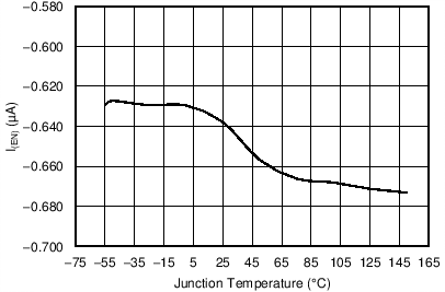
| Input current | Enable threshold 50 mV | –3.8 | μA | ||||
| Enable threshold –50 mV | –0.9 | ||||||
| Hysteresis current | –2.9 | μA | |||||
| VOLTAGE REFERENCE | |||||||
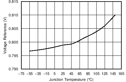
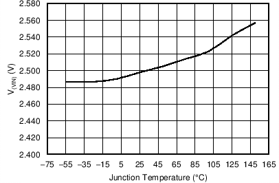
| Voltage reference | TJ = 25°C | 0.792 | 0.8 | 0.808 | V | ||
| 0.78 | 0.8 | 0.821 | |||||
| HIGH-SIDE MOSFET | |||||||
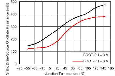
| On-resistance | V(VIN) = 3.5 V, BOOT-PH = 3 V | 300 | mΩ | ||||
| V(VIN) = 12 V, BOOT-PH = 6 V | 200 | 465 | |||||
| ERROR AMPLIFIER | |||||||
| Input current | 50 | nA | |||||
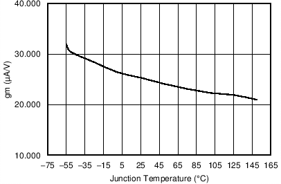
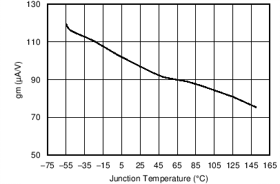
| Error amplifier transconductance (gM) | –2 μA < ICOMP < 2 μA, VCOMP = 1 V | 97 | μMhos | ||||
| Error amplifier transconductance (gM) during slow start | –2 μA < ICOMP < 2 μA, VCOMP = 1 V, V(VSENSE) = 0.4 V |
26 | μMhos | ||||
| Error amplifier dc gain | V(VSENSE) = 0.8 V | 10000 | V/V | ||||
| Error amplifier bandwidth | 2700 | kHz | |||||
| Error amplifier source/sink | V(COMP) = 1 V, 100 mV overdrive | ±7 | μA | ||||
| COMP to switch current transconductance | 1.9 | A/V | |||||
| CURRENT LIMIT | |||||||
| Current limit threshold | V(VIN) = 12 V | 0.5 | 0.94 | A | |||
| THERMAL SHUTDOWN | |||||||
| Thermal shutdown | 182 | °C | |||||
| TIMING RESISTOR AND EXTERNAL CLOCK (RT/CLK PIN) | |||||||
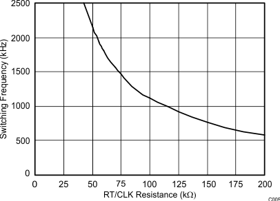
| Switching frequency range using RT mode | V(VIN) = 12 V | 130 | 2500 | kHz | |||
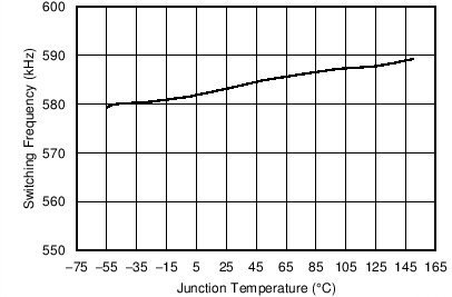
| ƒSW | Switching frequency | V(VIN) = 12 V, RT = 200 kΩ | 440 | 581 | 740 | kHz | |
| Switching frequency range using CLK mode | V(VIN) = 12 V | 300 | 2200 | kHz | |||
| Minimum CLK input pulse width | 40 | ns | |||||
| RT/CLK high threshold | V(VIN) = 12 V | 1.9 | 2.2 | V | |||
| RT/CLK low threshold | V(VIN) = 12 V | 0.5 | 0.7 | V | |||
| RT/CLK falling edge to PH rising edge delay | Measured at 500 kHz with RT resistor in series | 60 | ns | ||||
| PLL lock in time | Measured at 500 kHz | 100 | μs | ||||
| SLOW START AND TRACKING (SS/TR) | |||||||
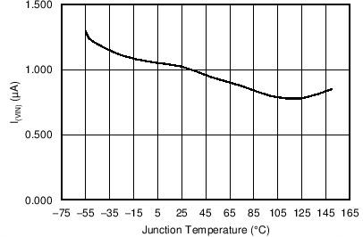
| Charge current | V(SS/TR) = 0.4 V | 2 | μA | ||||
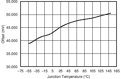
| SS/TR-to-VSENSE matching | V(SS/TR) = 0.4 V | 45 | mV | ||||
| SS/TR-to-reference crossover | 98% nominal | 1.0 | V | ||||
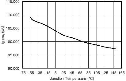
| SS/TR discharge current (overload) | V(VSENSE) = 0 V, V(SS/TR) = 0.4 V | 112 | μA | ||||
| SS/TR discharge voltage | V(VSENSE) = 0 V | 54 | mV | ||||
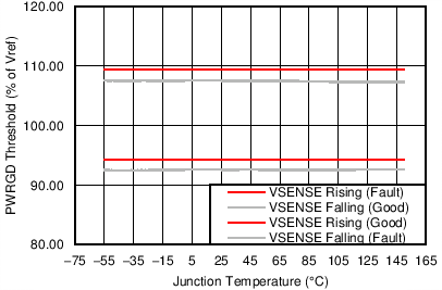
| POWER GOOD (PWRGD PIN) | |||||||
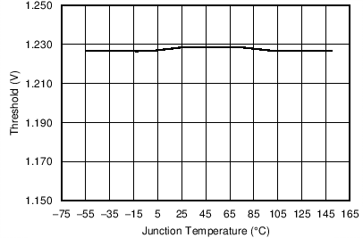
| V(VSENSE) | VSENSE threshold | VSENSE falling (fault) | 92% | ||||
| VSENSE rising (good) | 94% | ||||||
| VSENSE rising (fault) | 109% | ||||||
| VSENSE falling (good) | 107% | ||||||
| Hysteresis | VSENSE falling | 2% | |||||
| Output high leakage | V(VSENSE) = VREF, V(PWRGD) = 5.5 V, 25°C | 10 | nA | ||||
| On resistance | I(PWRGD) = 3 mA, V(VSENSE) < 0.79 V | 50 | Ω | ||||
| Minimum VIN for defined output | V(PWRGD) < 0.5 V, I(PWRGD) = 100 μA | 0.95 | 1.5 | V | |||
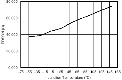
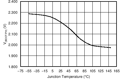
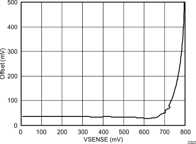
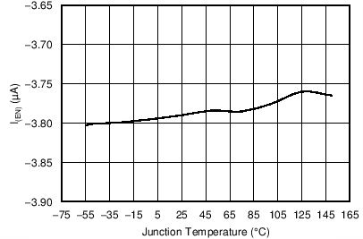
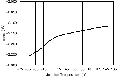
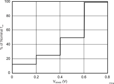
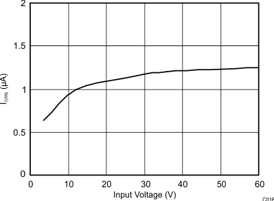
7.6 Typical Characteristics
| VIN = 12 V |
| VIN = 12 V |
| VIN = 12 V | TJ = 25°C |
| VIN = 12 V |
| VIN = 12 V |
| VIN = 12 V | V(EN) = Threshold –50 mV | |
| VIN = 12 V | ||
| VIN = 12 V | ||
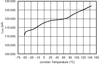
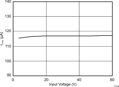
| VIN = 12 V | V(VSENSE) = 0.83 V | |
| VIN = 12 V |
| VIN = 12 V | TJ = 25°C |
| VIN = 12 V |
| VIN = 12 V | RT = 200 kΩ |
| VIN = 12 V | TJ = 25°C |
| VIN = 12 V |
| VIN = 12 V | V(EN) = Threshold 50 mV | |
| VIN = 12 V |
| VIN = 12 V | TJ = 25°C |
| TJ = 25°C |
| TJ = 25°C | V(VSENSE) = 0.83 V | |
| VIN = 12 V |
| VIN = 12 mV | V(SS/TR) = 0.2 V | |