SLVSCF8 July 2014 TPS54060-EP
PRODUCTION DATA.
- 1 Features
- 2 Applications
- 3 Description
- 4 Simplified Schematic
- 5 Revision History
- 6 Pin Configuration and Functions
- 7 Specifications
-
8 Detailed Description
- 8.1 Overview
- 8.2 Functional Block Diagram
- 8.3
Feature Description
- 8.3.1 Fixed Frequency PWM Control
- 8.3.2 Slope Compensation Output Current
- 8.3.3 Low-Dropout Operation and Bootstrap Voltage (Boot)
- 8.3.4 Error Amplifier
- 8.3.5 Voltage Reference
- 8.3.6 Adjusting the Output Voltage
- 8.3.7 Enable and Adjusting UVLO
- 8.3.8 Slow Start/Tracking Pin (SS/TR)
- 8.3.9 Overload Recovery Circuit
- 8.3.10 Sequencing
- 8.3.11 Constant Switching Frequency and Timing Resistor (RT/CLK Pin)
- 8.3.12 Overcurrent Protection and Frequency Shift
- 8.3.13 Selecting the Switching Frequency
- 8.3.14 How to Interface to RT/CLK Pin
- 8.3.15 Power Good (PWRGD Pin)
- 8.3.16 Overvoltage Transient Protection (OVTP)
- 8.3.17 Thermal Shutdown
- 8.3.18 Small Signal Model for Loop Response
- 8.3.19 Simple Small Signal Model for Peak Current Mode Control
- 8.3.20 Small Signal Model for Frequency Compensation
- 8.4 Device Functional Modes
-
9 Application and Implementation
- 9.1 Application Information
- 9.2
Typical Application
- 9.2.1 Design Requirements
- 9.2.2
Detailed Design Procedure
- 9.2.2.1 Selecting the Switching Frequency
- 9.2.2.2 Output Inductor Selection (LO)
- 9.2.2.3 Output Capacitor
- 9.2.2.4 Catch Diode
- 9.2.2.5 Input Capacitor
- 9.2.2.6 Slow Start Capacitor
- 9.2.2.7 Bootstrap Capacitor Selection
- 9.2.2.8 UVLO Set Point
- 9.2.2.9 Output Voltage and Feedback Resistors Selection
- 9.2.2.10 Compensation
- 9.2.3 Application Curves
- 10Power Supply Recommendations
- 11Layout
- 12Device and Documentation Support
- 13Mechanical, Packaging, and Orderable Information
Package Options
Mechanical Data (Package|Pins)
- DGQ|10
Thermal pad, mechanical data (Package|Pins)
- DGQ|10
Orderable Information
10 Power Supply Recommendations
10.1 Power Dissipation Estimate
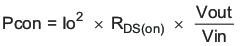
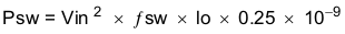
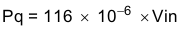
The following formulas show how to estimate the IC power dissipation under CCM operation. Do not use these equations if the device is working in DCM.
The power dissipation of the IC includes conduction loss (Pcon), switching loss (Psw), gate drive loss (Pgd), and supply current (Pq).

where:
- IOUT is the output current (A).
- RDS(on) is the on-resistance of the high-side MOSFET (Ω).
- VOUT is the output voltage (V).
- VIN is the input voltage (V).
- ƒsw is the switching frequency (Hz).
So

For given TA,

For given TJMAX = 150°C

where
- Ptot is the total device power dissipation (W).
- TA is the ambient temperature (°C).
- TJ is the junction temperature (°C).
- Rth is the thermal resistance of the package (°C/W).
- TJMAX is maximum junction temperature (°C).
- TAMAX is maximum ambient temperature (°C).
There will be additional power losses in the regulator circuit due to the inductor AC and DC losses, catch diode, and trace resistance that will impact the overall efficiency of the regulator.
10.2 Power Supply Considerations
TPS2105-EP requires a high-quality ceramic, type X5R or X7R, input decoupling capacitor. The value of a ceramic capacitor varies significantly over temperature and the amount of DC bias applied to the capacitor. The capacitance variations due to temperature can be minimized by selecting a dielectric material that is stable over temperature. X5R and X7R ceramic dielectrics are usually selected for power regulator capacitors because they have a high capacitance to volume ratio and are fairly stable over temperature. The output capacitor must also be selected with the DC bias taken into account. Ceramic capacitors lose capacitance when a DC bias is applied across the capacitor. This capacitance loss is due to the polarization of the ceramic material. The capacitance loss is not permanent; after a large DC bias is applied, reducing the DC bias reduces the degree of polarization and capacitance increases. The capacitance value of a capacitor decreases as the DC bias across a capacitor increases.
All tantalum capacitors have Tantalum (Ta) particles sintered together to form an anode. The cathode material can either be the traditional MnO2 or a conductive polymer. Because MnO2 is actually a semiconductor, it has a very-high amount of resistance associated with it. A characteristic of this material is that as temperature changes so does its conductivity. So MnO2-based Tantalum capacitors have relatively high ESR and that ESR shifts significantly across the operational temperature range.
However, polymer-based cathodes use a highly-conductive polymer material. Because the material is inherently conductive, Tantalum-polymers have a relatively low ESR compared to their MnO2 counterparts in the same voltage and capacitance ranges.
All Tantalum capacitors have a voltage derating factor associated with them. Because the Polymer material puts less stress on the Tantalum-Pentoxide dielectric during reflow soldering, more voltage can be applied compared to a MnO2-based Tantalum. For polymer-based capacitors, TI recommends 20% derating whereas the MnO2-based tantalum capacitors require 50% or higher derating. Refer to the capacitor vendor data sheet for more details regarding the derating guidelines.