SLVSAV1D May 2011 – July 2016 TPS54062
PRODUCTION DATA.
- 1 Features
- 2 Applications
- 3 Description
- 4 Revision History
- 5 Pin Configuration and Functions
- 6 Specifications
-
7 Detailed Description
- 7.1 Overview
- 7.2 Functional Block Diagram
- 7.3
Feature Description
- 7.3.1 Fixed-Frequency PWM Control
- 7.3.2 Slope Compensation Output Current
- 7.3.3 Error Amplifier
- 7.3.4 Voltage Reference
- 7.3.5 Adjusting the Output Voltage
- 7.3.6 Enable and Adjusting Undervoltage Lockout
- 7.3.7 Constant Switching Frequency and Timing Resistor (RT/CLK Pin)
- 7.3.8 Selecting the Switching Frequency
- 7.3.9 How to Interface to RT/CLK Pin
- 7.3.10 Overvoltage Transient Protection
- 7.3.11 Thermal Shutdown
- 7.4 Device Functional Modes
-
8 Applications and Implementation
- 8.1 Application Information
- 8.2
Typical Applications
- 8.2.1
Continuous Conduction Mode (CCM) Switching Regulator
- 8.2.1.1 Design Requirements
- 8.2.1.2
Detailed Design Procedure
- 8.2.1.2.1 Selecting the Switching Frequency
- 8.2.1.2.2 Output Inductor Selection (LO)
- 8.2.1.2.3 Output Capacitor
- 8.2.1.2.4 Input capacitor
- 8.2.1.2.5 Bootstrap Capacitor Selection
- 8.2.1.2.6 Under Voltage Lock Out Set Point
- 8.2.1.2.7 Output Voltage and Feedback Resistors Selection
- 8.2.1.2.8 Closing the Loop
- 8.2.1.3 Application Curves
- 8.2.2 DCM Application
- 8.2.1
Continuous Conduction Mode (CCM) Switching Regulator
- 9 Power Supply Recommendations
- 10Layout
- 11Device and Documentation Support
- 12Mechanical, Packaging, and Orderable Information
Package Options
Mechanical Data (Package|Pins)
Thermal pad, mechanical data (Package|Pins)
- DRB|8
Orderable Information
1 Features
- Integrated High-Side and Low-Side MOSFET
- Peak Current Mode Control
- Diode Emulation for Improved Light-Load Efficiency
- 89 µA (typical) Operating Quiescent Current
- 100-kHz to 400-kHz Adjustable Switching Frequency
- Synchronizes to External Clock
- Internal Slow-Start
- 0.8 V ±2% Voltage Reference
- Stable with Ceramic Output Capacitors or Low-Cost Aluminum Electrolytic
- Cycle-by-Cycle Current Limit, Thermal and Frequency Foldback Protection
- MSOP-8 and 3mm × 3mm VSON-8 Packages
2 Applications
- Low-Power Standby or Bias Voltage Supplies
- 4-20 mA Current-Loop Powered Sensors
- Industrial Process Control, Metering, and Security Systems
- High Voltage Linear Regulator Replacement
3 Description
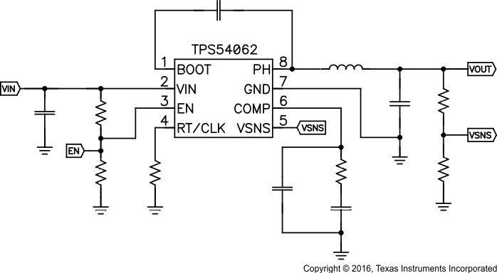
The TPS54062 device is a 60-V, 50-mA, synchronous step-down converter with integrated high-side and low-side MOSFETs. Current mode control provides simple external compensation and flexible component selection. The non-switching supply current is 89 µA. Using the enable pin, shutdown supply current is reduced to 1.7 µA.
Undervoltage lockout is internally set at 4.5 V, but can be increased using the accurate enable pin threshold. The output voltage start-up ramp is controlled by the internal slow-start time.
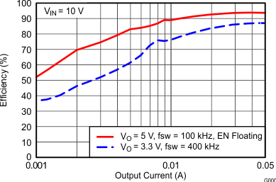
Adjustable switching frequency range allows efficiency and external component size to be optimized. Frequency foldback and thermal shutdown protects the part during an overload condition.
Device Information(1)
| PART NUMBER | PACKAGE | BODY SIZE (NOM) |
|---|---|---|
| TPS54062 | MSOP (8) | 3.00 mm × 3.00 mm |
| VSON (8) |
- For all available packages, see the orderable addendum at the end of the datasheet.

