SLVS889C October 2008 – November 2014 TPS54140
PRODUCTION DATA.
- 1 Features
- 2 Applications
- 3 Description
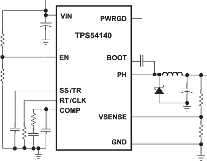
- 4 Simplified Schematic
- 5 Revision History
- 6 Pin Configuration and Functions
- 7 Specifications
-
8 Detailed Description
- 8.1 Overview
- 8.2 Functional Block Diagram
- 8.3
Feature Description
- 8.3.1 Fixed Frequency PWM Control
- 8.3.2 Slope Compensation Output Current
- 8.3.3 Bootstrap Voltage (BOOT)
- 8.3.4 Low Dropout Operation
- 8.3.5 Error Amplifier
- 8.3.6 Voltage Reference
- 8.3.7 Adjusting the Output Voltage
- 8.3.8 Enable and Adjusting Undervoltage Lockout
- 8.3.9 Slow Start and Tracking Pin (SS/TR)
- 8.3.10 Overload-Recovery Circuit
- 8.3.11 Sequencing
- 8.3.12 Constant Switching Frequency and Timing Resistor (RT/CLK Pin)
- 8.3.13 Overcurrent Protection and Frequency Shift
- 8.3.14 Selecting the Switching Frequency
- 8.3.15 How to Interface to RT/CLK Pin
- 8.3.16 Power Good (PWRGD Pin)
- 8.3.17 Overvoltage Transient Protection
- 8.3.18 Thermal Shutdown
- 8.3.19 Small-Signal Model for Loop Response
- 8.3.20 Simple Small-Signal Model for Peak-Current Mode Control
- 8.3.21 Small-Signal Model for Frequency Compensation
- 8.4 Device Functional Modes
-
9 Application and Implementation
- 9.1 Application Information
- 9.2
Typical Application
- 9.2.1 Design Requirements
- 9.2.2
Detailed Design Procedure
- 9.2.2.1 Selecting the Switching Frequency
- 9.2.2.2 Output Inductor Selection (LO)
- 9.2.2.3 Output Capacitor
- 9.2.2.4 Catch Diode
- 9.2.2.5 Input Capacitor
- 9.2.2.6 Slow-Start Capacitor
- 9.2.2.7 Bootstrap Capacitor Selection
- 9.2.2.8 Undervoltage-Lockout Set Point
- 9.2.2.9 Output Voltage and Feedback Resistors Selection
- 9.2.2.10 Compensation
- 9.2.2.11 Power Dissipation Estimate
- 9.2.3 Application Curves
- 10Power Supply Recommendations
- 11Layout
- 12Device and Documentation Support
- 13Mechanical, Packaging, and Orderable Information
Package Options
Mechanical Data (Package|Pins)
- DGQ|10
Thermal pad, mechanical data (Package|Pins)
- DGQ|10
Orderable Information
1 Features
- 3.5- to 42-V Input Voltage Range
- 200-mΩ High-Side MOSFET
- High Efficiency at Light Loads with a Pulse Skipping Eco-mode™
- 116-μA Operating Quiescent Current
- 1.3-μA Shutdown Current
- 100-kHz to 2.5-MHz Switching Frequency
- Synchronizes to External Clock
- Adjustable Slow Start and Sequencing
- UV and OV Power-Good Output
- Adjustable UVLO Voltage and Hysteresis
- 0.8-V Internal Voltage Reference
- MSOP10 Package With PowerPAD™
- Supported by WEBENCH® Software Tool (www.TI.com/WEBENCH)
2 Applications
- 12-V and 24-V Industrial and Commercial Low Power Systems
- Aftermarket Auto Accessories: Video, GPS, Entertainment
3 Description
The TPS54140 device is a 42-V, 1.5-A, step-down regulator with an integrated high-side MOSFET. Current mode control provides simple external compensation and flexible component selection. A low-ripple pulse-skip mode reduces the no load, regulated output-supply current to 116 μA. Using the enable pin, the shutdown supply current is reduced to 1.3 μA.
Undervoltage lockout is internally set at 2.5 V, but can be increased using the enable pin. The output-voltage startup ramp is controlled by the slow-start pin that can also be configured for sequencing and tracking. An open-drain power-good signal indicates the output is within 94% to 107% of the nominal voltage.
A wide switching frequency range allows efficiency and external component size to be optimized. Frequency foldback and thermal shutdown protects the device during an overload condition.
The TPS54140 device is available in a 10-pin thermally enhanced MSOP PowerPAD package.
Device Information(1)
| PART NUMBER | PACKAGE | BODY SIZE (NOM) |
|---|---|---|
| TPS54140 | MSOP (10) | 3.00 mm × 3.00 mm |
- For all available packages, see the orderable addendum at the end of the datasheet.
4 Simplified Schematic
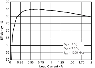
Efficiency vs Load Current