SLVS889C October 2008 – November 2014 TPS54140
PRODUCTION DATA.
- 1 Features
- 2 Applications
- 3 Description
- 4 Simplified Schematic
- 5 Revision History
- 6 Pin Configuration and Functions
- 7 Specifications
-
8 Detailed Description
- 8.1 Overview
- 8.2 Functional Block Diagram
- 8.3
Feature Description
- 8.3.1 Fixed Frequency PWM Control
- 8.3.2 Slope Compensation Output Current
- 8.3.3 Bootstrap Voltage (BOOT)
- 8.3.4 Low Dropout Operation
- 8.3.5 Error Amplifier
- 8.3.6 Voltage Reference
- 8.3.7 Adjusting the Output Voltage
- 8.3.8 Enable and Adjusting Undervoltage Lockout
- 8.3.9 Slow Start and Tracking Pin (SS/TR)
- 8.3.10 Overload-Recovery Circuit
- 8.3.11 Sequencing
- 8.3.12 Constant Switching Frequency and Timing Resistor (RT/CLK Pin)
- 8.3.13 Overcurrent Protection and Frequency Shift
- 8.3.14 Selecting the Switching Frequency
- 8.3.15 How to Interface to RT/CLK Pin
- 8.3.16 Power Good (PWRGD Pin)
- 8.3.17 Overvoltage Transient Protection
- 8.3.18 Thermal Shutdown
- 8.3.19 Small-Signal Model for Loop Response
- 8.3.20 Simple Small-Signal Model for Peak-Current Mode Control
- 8.3.21 Small-Signal Model for Frequency Compensation
- 8.4 Device Functional Modes
-
9 Application and Implementation
- 9.1 Application Information
- 9.2
Typical Application
- 9.2.1 Design Requirements
- 9.2.2
Detailed Design Procedure
- 9.2.2.1 Selecting the Switching Frequency
- 9.2.2.2 Output Inductor Selection (LO)
- 9.2.2.3 Output Capacitor
- 9.2.2.4 Catch Diode
- 9.2.2.5 Input Capacitor
- 9.2.2.6 Slow-Start Capacitor
- 9.2.2.7 Bootstrap Capacitor Selection
- 9.2.2.8 Undervoltage-Lockout Set Point
- 9.2.2.9 Output Voltage and Feedback Resistors Selection
- 9.2.2.10 Compensation
- 9.2.2.11 Power Dissipation Estimate
- 9.2.3 Application Curves
- 10Power Supply Recommendations
- 11Layout
- 12Device and Documentation Support
- 13Mechanical, Packaging, and Orderable Information
Package Options
Mechanical Data (Package|Pins)
- DGQ|10
Thermal pad, mechanical data (Package|Pins)
- DGQ|10
Orderable Information
6 Pin Configuration and Functions
DGQ Package
10-Pin MSOP With PowerPAD™
Top View
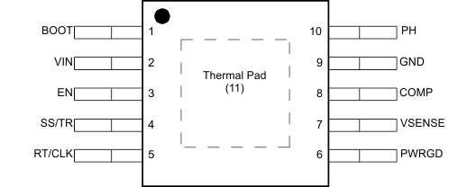
Pin Functions
| PIN | I/O | DESCRIPTION | ||
|---|---|---|---|---|
| NO. | NAME | |||
| 1 | BOOT | O | A bootstrap capacitor is required between the BOOT and PH pins. If the voltage on this capacitor is below the minimum required by the device, the output is forced to switch off until the capacitor is refreshed. | |
| 2 | VIN | I | This pin is the 3.5- to 42-V input supply voltage. | |
| 3 | EN | I | This pin is the enable pin and internal pullup current source. To disable, pull below 1.2 V. Float this pin to enable. Adjust the input undervoltage lockout with two resistors. | |
| 4 | SS/TR | I | This pin is the slow-start and tracking pin. An external capacitor connected to this pin sets the output rise time. Because the voltage on this pin overrides the internal reference, it can be used for tracking and sequencing. | |
| 5 | RT/CLK | I | This pin is the resistor timing and external clock pin. An internal amplifier holds this pin at a fixed voltage when using an external resistor to ground to set the switching frequency. If the pin is pulled above the PLL upper threshold, a mode change occurs and the pin becomes a synchronization input. The internal amplifier is disabled and the pin is a high impedance clock input to the internal PLL. If clocking edges stop, the internal amplifier is re-enabled and the mode returns to a resistor set function. | |
| 6 | PWRGD | O | This pin is an open drain output. This pin is asserted low if the output voltage is low because of thermal shutdown, dropout, overvoltage, or EN shut down. | |
| 7 | VSENSE | I | This pin is the inverting node of the transconductance (gm) error amplifier. | |
| 8 | COMP | O | This pin is the error amplifier output and input to the output-switch current comparator. Connect frequency compensation components to this pin. | |
| 9 | GND | — | Ground pin | |
| 10 | PH | O | This pin is the source of the internal high-side power MOSFET. | |
| 11 | Thermal Pad | — | The GND pin must be electrically connected to the exposed pad on the printed circuit board for proper operation. | |