SLVS889C October 2008 – November 2014 TPS54140
PRODUCTION DATA.
- 1 Features
- 2 Applications
- 3 Description
- 4 Simplified Schematic
- 5 Revision History
- 6 Pin Configuration and Functions
- 7 Specifications
-
8 Detailed Description
- 8.1 Overview
- 8.2 Functional Block Diagram
- 8.3
Feature Description
- 8.3.1 Fixed Frequency PWM Control
- 8.3.2 Slope Compensation Output Current
- 8.3.3 Bootstrap Voltage (BOOT)
- 8.3.4 Low Dropout Operation
- 8.3.5 Error Amplifier
- 8.3.6 Voltage Reference
- 8.3.7 Adjusting the Output Voltage
- 8.3.8 Enable and Adjusting Undervoltage Lockout
- 8.3.9 Slow Start and Tracking Pin (SS/TR)
- 8.3.10 Overload-Recovery Circuit
- 8.3.11 Sequencing
- 8.3.12 Constant Switching Frequency and Timing Resistor (RT/CLK Pin)
- 8.3.13 Overcurrent Protection and Frequency Shift
- 8.3.14 Selecting the Switching Frequency
- 8.3.15 How to Interface to RT/CLK Pin
- 8.3.16 Power Good (PWRGD Pin)
- 8.3.17 Overvoltage Transient Protection
- 8.3.18 Thermal Shutdown
- 8.3.19 Small-Signal Model for Loop Response
- 8.3.20 Simple Small-Signal Model for Peak-Current Mode Control
- 8.3.21 Small-Signal Model for Frequency Compensation
- 8.4 Device Functional Modes
-
9 Application and Implementation
- 9.1 Application Information
- 9.2
Typical Application
- 9.2.1 Design Requirements
- 9.2.2
Detailed Design Procedure
- 9.2.2.1 Selecting the Switching Frequency
- 9.2.2.2 Output Inductor Selection (LO)
- 9.2.2.3 Output Capacitor
- 9.2.2.4 Catch Diode
- 9.2.2.5 Input Capacitor
- 9.2.2.6 Slow-Start Capacitor
- 9.2.2.7 Bootstrap Capacitor Selection
- 9.2.2.8 Undervoltage-Lockout Set Point
- 9.2.2.9 Output Voltage and Feedback Resistors Selection
- 9.2.2.10 Compensation
- 9.2.2.11 Power Dissipation Estimate
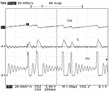
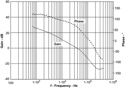
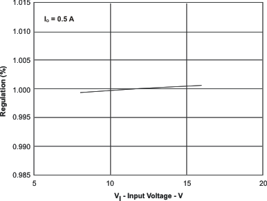
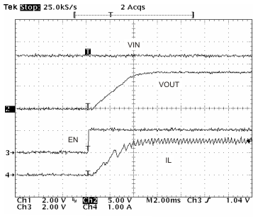
- 9.2.3 Application Curves
- 10Power Supply Recommendations
- 11Layout
- 12Device and Documentation Support
- 13Mechanical, Packaging, and Orderable Information
Package Options
Mechanical Data (Package|Pins)
- DGQ|10
Thermal pad, mechanical data (Package|Pins)
- DGQ|10
Orderable Information
9 Application and Implementation
NOTE
Information in the following applications sections is not part of the TI component specification, and TI does not warrant its accuracy or completeness. TI’s customers are responsible for determining suitability of components for their purposes. Customers should validate and test their design implementation to confirm system functionality.
9.1 Application Information
The TPS54140 device is typically used as a step-down converter, which converts a voltage from 3.5 V to 42 V to a lower voltage. WEBENCH software is available to aid in the design and analysis of circuits.
9.2 Typical Application
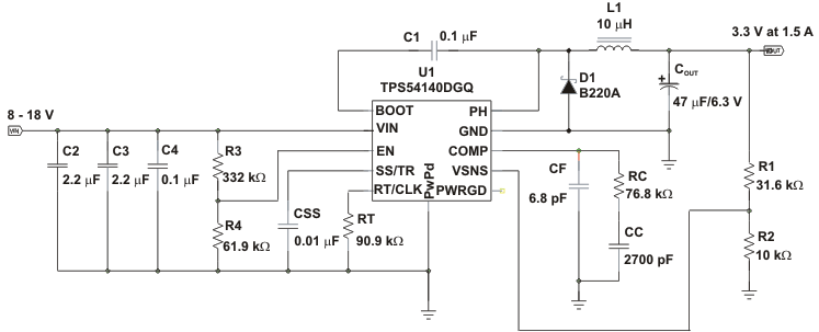 Figure 50. High Frequency, 3.3-V Output Power Supply Design With Adjusted UVLO
9.2.1 Design Requirements
For this design example, use the parameters listed in Table 1 as the input parameters.
Table 1. Design Parameters
9.2.2 Detailed Design Procedure
This example details the design of a high-frequency switching-regulator design using ceramic output capacitors. A few parameters must be known to start the design process. These parameters are typically determined at the system level.
9.2.2.1 Selecting the Switching Frequency
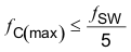
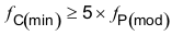
The first step of the design process is to decide on a switching frequency for the regulator. Typically, the user selects the highest switching frequency possible because it produces the smallest solution size. The high switching frequency allows for lower valued inductors and smaller output capacitors compared to a power supply that switches at a lower frequency. The switching frequency that can be selected is limited by the minimum on-time of the internal power switch, the input voltage, and the output voltage and the frequency shift limitation.
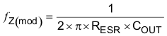
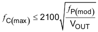
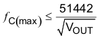
Equation 12 and Equation 13 must be used to find the maximum switching frequency for the regulator. Select the lower value of the two equations. Switching frequencies higher than these values result in pulse skipping or the lack of overcurrent protection during a short circuit.
The typical minimum on time, tonmin, is 130 ns for the TPS54140 device. For this example, the output voltage is 3.3 V and the maximum input voltage is 18 V, which allows for a maximum switch frequency up to 1600 kHz when including the inductor resistance, on resistance, and diode voltage in Equation 12. To ensure that overcurrent runaway is not a concern during short circuits in the design use Equation 13 or the solid curve in Figure 40 to determine the maximum switching frequency. The maximum switching frequency is approximately 1600 kHz with a maximum input voltage of 20 V and assuming the following: a diode voltage of 0.5 V, inductor resistance of 100 mΩ, switch resistance of 200 mΩ, and an output current of 2.8 A.
Selecting the lower of the two values and adding some margin, a switching frequency of 1200 kHz is used. To determine the timing resistance for a given switching frequency, use Equation 11 or the curve in Figure 38.
The switching frequency is set by resistor Rt shown in Figure 50.
9.2.2.2 Output Inductor Selection (LO)
Use Equation 28 to calculate the minimum value of the output inductor.
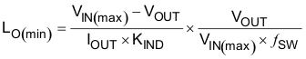
where
- KIND is a coefficient that represents the amount of inductor ripple current relative to the maximum output current
The inductor ripple current is filtered by the output capacitor. Therefore, selecting high inductor ripple currents impacts the selection of the output capacitor because the output capacitor must have a ripple current rating equal to or greater than the inductor ripple current. In general, the inductor ripple value is at the discretion of the designer; however, the following guidelines may be used.
For designs using low-ESR output capacitors such as ceramics, a value as high as KIND = 0.3 can be used. When using higher ESR output capacitors, KIND = 0.2 yields better results. Because the inductor ripple current is part of the PWM control system, the inductor ripple current should always be greater than 100 mA for dependable operation. In a wide input voltage regulator, selecting an inductor ripple current on the larger side is best which allows the inductor to still have a measurable ripple current with the input voltage at the minimum.
For this design example, use KIND = 0.2 and the minimum inductor value which is calculated as 7.6 μH. For this design, the nearest standard value of 10 μH was selected. For the output filter inductor, the RMS current and saturation current ratings must not be exceeded. Use Equation 30 to calculate the inductor ripple current, IRIPPLE.
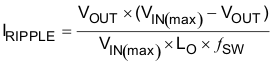
Use Equation 30 to calculate the RMS inductor current, IL(rms).
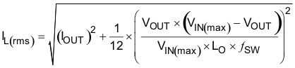
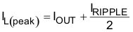
Use Equation 31 to calculate the peak inductor current.
For this design, the RMS inductor current is 1.506 A and the peak inductor current is 1.62 A. The selected inductor is a MSS6132-103 and has a saturation current rating of 1.64 A and an RMS current rating of 1.9 A.
As the equation set demonstrates, lower ripple currents reduce the output voltage ripple of the regulator but require a larger value of inductance. Selecting higher ripple currents increases the output voltage ripple of the regulator but allows for a lower inductance value.
The current flowing through the inductor is the inductor ripple current plus the output current. During power up, faults, or transient load conditions, the inductor current can increase above the peak-inductor current level that was calculated using Equation 31. In transient conditions, the inductor current can increase up to the switch current limit of the device. For this reason, the most conservative approach is to specify an inductor with a saturation-current rating equal to or greater than the switch current limit rather than the peak inductor current.
9.2.2.3 Output Capacitor
Consider three primary factors when selecting the value of the output capacitor. The output capacitor determines the modulator pole, the output voltage ripple, and how the regulator responds to a large change in load current. The output capacitance must be selected based on the more stringent of these three criteria.
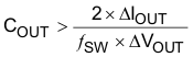
The desired response to a large change in the load current is the first criterion. The output capacitor must supply the load with current when the regulator cannot. This situation occurs if the desired hold-up times are present for the regulator. In this case, the output capacitor must hold the output voltage above a certain level for a specified amount of time after the input power is removed. The regulator is also temporarily unable to supply sufficient output current if a large, fast increase occurs affecting the current requirements of the load, such as a transition from no load to full load. The regulator usually requires two or more clock cycles for the control loop to notice the change in load current and output voltage and to adjust the duty cycle to react to the change. The output capacitance must be large enough to supply the difference in current for 2 clock cycles while only allowing a tolerable amount of droop in the output voltage. Use Equation 32 to calculate the minimum output capacitance required to supply the difference in current.
where
- ΔIOUT is the change in output current
- ƒSW is the regulators switching frequency
- ΔVOUT is the allowable change in the output voltage
For this example, the transient load response is specified as a 4% change in VOUT for a load step from 0 A (no load) to 1.5 A (full load). For this example, ΔIOUT = 1.5 – 0 = 1.5 A and ΔVOUT = 0.04 × 3.3 = 0.132 V. Using these values results in a minimum capacitance of 18.9 μF. This value does not consider the ESR of the output capacitor in the output voltage change. For ceramic capacitors, the ESR is usually small enough to ignore in this calculation. Aluminum electrolytic and tantalum capacitors have higher ESR which should be taken into consideration.
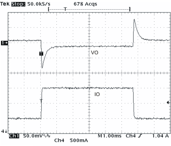
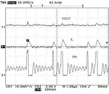
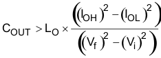
The catch diode of the regulator cannot sink current and therefore any stored energy in the inductor produces an output-voltage overshoot when the load current rapidly decreases (see Figure 51). The output capacitor must also be sized to absorb energy stored in the inductor when transitioning from a high load current to a lower load current. The excess energy that is stored in the output capacitor increases the voltage on the capacitor. The capacitor must be sized to maintain the desired output voltage during these transient periods. Use Equation 33 to calculate the minimum capacitance to keep the output voltage overshoot to a desired value.
where
- L is the value of the inductor
- IOH is the output current under heavy load
- IOL is the output under light load
- Vf is the final peak output voltage
- Vi is the initial capacitor voltage
For this example, the worst-case load step is be from 1.5 A to 0 A. The output voltage increases during this load transition and the stated maximum in the specification is 4% of the output voltage. Therefore Vf = 1.04 × 3.3 = 3.432. The initial capacitor voltage, Vi, is the nominal output voltage of 3.3 V. Using these values in Equation 33 yields a minimum capacitance of 25.3 μF.
Use Equation 34 to calculate the minimum output capacitance required to meet the output voltage ripple specification.
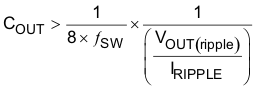
where
- ƒSW is the switching frequency
- VOUT(ripple) is the maximum allowable output voltage ripple
- IRIPPLE is the inductor ripple current
Equation 35 yields 0.7μF.
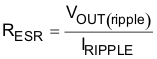
Use Equation 35 to calculate the maximum ESR an output capacitor can have to meet the output-voltage ripple specification. Equation 35 indicates the ESR should be less than 144 mΩ.
The most stringent criterion for the output capacitor is 25.3 μF of capacitance to maintain the output voltage in regulation during an unload transient.
Additional capacitance deratings for aging, temperature, and DC bias should be considered which increases this minimum value. For this example, a 47-μF 6.3-V X7R ceramic capacitor with 5 mΩ of ESR is used.
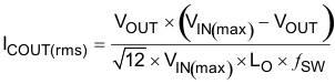
Capacitors generally have limits to the amount of ripple current they can handle without failing or producing excess heat. An output capacitor that can support the inductor ripple current must be specified. Some capacitor data sheets specify the root-mean-square (RMS) value of the maximum ripple current. Use Equation 36 to calculate the RMS ripple current that the output capacitor must support. For this application, Equation 36 yields 66 mA.
9.2.2.4 Catch Diode
The TPS54140 device requires an external catch diode between the PH and GND pins. The selected diode must have a reverse voltage rating equal to or greater than VIN(max). The peak current rating of the diode must be greater than the maximum inductor current. The diode should also have a low forward voltage. Schottky diodes are typically a good choice for the catch diode because of the low forward voltage of these diodes. The lower the forward voltage of the diode, the higher the efficiency of the regulator will be.
Typically, the higher the voltage and current ratings of the diode, the higher the forward voltage will be. Because the design example has an input voltage up to 18 V, a diode with a minimum of 20-V reverse voltage is selected.
For the example design, the B220A Schottky diode is selected because of the lower forward voltage and because it comes in a larger package size which has good thermal characteristics over small devices. The typical forward voltage of the B220A is 0.5 V.
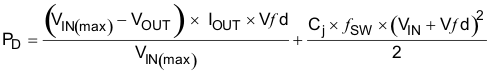
The diode must also be selected with an appropriate power rating. The diode conducts the output current during the off-time of the internal power switch. The off-time of the internal switch is a function of the maximum input voltage, the output voltage, and the switching frequency. The output current during the off-time is multiplied by the forward voltage of the diode which equals the conduction losses of the diode. At higher switch frequencies, the AC losses of the diode must be considered. The AC losses of the diode are because of the charging and discharging of the junction capacitance and reverse recovery. Use Equation 37 to calculate the total power dissipation, conduction losses, and AC losses of the diode.
The B220A diode has a junction capacitance of 120 pF. Using Equation 37, the selected diode dissipates 0.632 W. Depending on mounting techniques, this power dissipation should produce a 16°C temperature rise in the diode when the input voltage is 18 V and the load current is 1.5 A.
If the power supply spends a significant amount of time at light-load currents or in sleep mode, consider using a diode that has a low leakage current and slightly-higher forward-voltage drop.
9.2.2.5 Input Capacitor
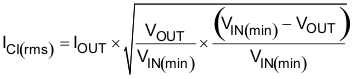
The TPS54140 device requires a high-quality ceramic, type X5R or X7R, input decoupling capacitor with an effective capacitance value of at least 3 μF and in some applications additional bulk capacitance. The effective capacitance includes any DC bias effects. The voltage rating of the input capacitor must be greater than the maximum input voltage. The capacitor must also have a ripple-current rating greater than the maximum input current ripple of the TPS54140 device. Use Equation 38 to calculate the input ripple current, ICI(rms).
The value of a ceramic capacitor varies significantly over temperature and the amount of DC bias applied to the capacitor. The capacitance variations because temperature can be minimized by selecting a dielectric material that is stable over temperature. X5R and X7R ceramic dielectrics are usually selected for power-regulator capacitors because these dielectrics have a high capacitance-to-volume ratio and are fairly stable over temperature. The output capacitor must also be selected with the DC bias taken into account. The capacitance value of a capacitor decreases as the DC bias across a capacitor increases.
For this example design, a ceramic capacitor with at least a 20-V voltage rating is required to support the maximum input voltage. Common standard ceramic-capacitor voltage ratings include 4 V, 6.3 V, 10 V, 16 V, 25 V, 50 V, or 100 V. Therefore, a 25-V capacitor should be selected. For this example, two 2.2-μF, 25-V capacitors in parallel have been selected. Table 2 lists a selection of high-voltage capacitors. The input capacitance value determines the input ripple voltage of the regulator. Use Equation 39 to calculate the input voltage ripple.
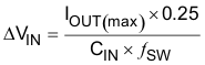
Using the design example values, IOUT(max) = 1.5 A, CIN = 4.4 μF, ƒSW = 1200 kHz, yields an input voltage ripple of 71 mV and an RMS input ripple current of 0.701 A.
Table 2. Capacitor Types
| VENDOR | VALUE (μF) | EIA Size | VOLTAGE (V) | DIALECTRIC | COMMENTS |
|---|---|---|---|---|---|
| Murata | 1 to 2.2 | 1210 | 100 | X7R | GRM32 series |
| 1 to 4.7 | 50 | ||||
| 1 | 1206 | 100 | GRM31 series | ||
| 1 to 2.2 | 50 | ||||
| Vishay | 1 to 1.8 | 2220 | 50 | VJ X7R series | |
| 1 to 1.2 | 100 | ||||
| 1 to 3.9 | 2225 | 50 | |||
| 1 to 1.8 | 100 | ||||
| TDK | 1 to 2.2 | 1812 | 100 | C series C4532 | |
| 1.5 to 6.8 | 50 | ||||
| 1 to 2.2 | 1210 | 100 | C series C3225 | ||
| 1 to 3.3 | 50 | ||||
| AVX | 1 to 4.7 | 1210 | 50 | X7R dielectric series | |
| 1 | 100 | ||||
| 1 to 4.7 | 1812 | 50 | |||
| 1 to 2.2 | 100 |
9.2.2.6 Slow-Start Capacitor
The slow-start capacitor determines the minimum amount of time required for the output voltage to reach the nominal programmed value during power up which is useful if a load requires a controlled-voltage slew rate. This feature is also used if the output capacitance is very large and requires large amounts of current to quickly charge the capacitor to the output voltage level. The large currents required to charge the capacitor may make the TPS54140 device reach the current limit, or excessive current draw from the input power supply may cause the input voltage rail to sag. Limiting the output-voltage slew rate solves both of these problems.
The slow-start time must be long enough to allow the regulator to charge the output capacitor up to the output voltage without drawing excessive current. Use Equation 40 to calculate the minimum slow-start time, tSS, required to charge the output capacitor, COUT, from 10% to 90% of the output voltage, VOUT, with an average slow start current of ISS(avg).
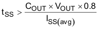
In the example, to charge the 47-μF output capacitor up to 3.3 V while only allowing the average input current to be 0.125 A requires a 1-ms slow-start time.
When the slow-start time is known, the slow-start capacitor value can be calculated using Equation 6. For the example circuit, the slow-start time is not too critical because the output capacitor value is 47 μF which does not require much current to charge to 3.3 V. The example circuit has the slow-start time set to an arbitrary value of 1 ms which requires a 3.3-nF capacitor.
9.2.2.7 Bootstrap Capacitor Selection
A 0.1-μF ceramic capacitor must be connected between the BOOT and PH pins for proper operation. Using a ceramic capacitor with X5R or better grade dielectric is recommended. The capacitor should have a 10-V or higher voltage rating.
9.2.2.8 Undervoltage-Lockout Set Point
The undervoltage lockout (UVLO) can be adjusted using an external voltage divider on the EN pin of the TPS54140 device. The UVLO has two thresholds, one for power up when the input voltage is rising and one for power down or brown outs when the input voltage is falling. For the example design, the supply should turn on and begin switching when the input voltage increases above 7.7 V (enabled). After the regulator begins switching, it should continue to do so until the input voltage falls below 6.7 V (UVLO stop).
The programmable UVLO and enable voltages are set using a resistor divider between VIN and ground to the EN pin. Equation 2 through Equation 3 can be used to calculate the resistance values necessary. For the example application, a 332 kΩ between VIN and EN and a 61.9 kΩ between EN and ground are required to produce the 7.7-V and 6.7-V start and stop voltages.
9.2.2.9 Output Voltage and Feedback Resistors Selection
For the example design, a value of 10 kΩ was selected for R2. Using Equation 1, the value of R1 is calculated as 31.25 kΩ. The nearest standard 1% resistor is 31.6 kΩ. Because of the current leakage of the VSENSE pin, the current flowing through the feedback network should be greater than 1 μA to maintain the output voltage accuracy. This requirement makes the maximum value of R2 equal to 800 kΩ. Selectinging higher resistor values decreases quiescent current and improves efficiency at low output currents but may introduce noise immunity problems.
9.2.2.10 Compensation
Several possible methods exist to design closed loop compensation for DC-DC converters. The method presented here yields high phase margins. For most conditions, the regulator has a phase margin between 60 and 90 degrees. The method presented here ignores the effects of the slope compensation that is internal to the TPS54140 device. Because the slope compensation is ignored, the actual crossover frequency is usually lower than the crossover frequency used in the calculations.
For a more accurate design use the WEBENCH software.
The uncompensated regulator has a dominant pole that is typically located between 300 Hz and 3 kHz because the output capacitor and load resistance and a pole from the error amplifier. One zero exists because of the output capacitor and the ESR. The zero frequency is higher than either of the two poles.
If left uncompensated, the double pole created by the error amplifier and the modulator can lead to an unstable regulator. To stabilize the regulator, one pole must be canceled out. One design approach is to locate a compensating zero at the modulator pole. Then select a crossover frequency that is higher than the modulator pole. The gain of the error amplifier can be calculated to achieve the desired crossover frequency. The capacitor used to create the compensation zero along with the output impedance of the error amplifier form a low frequency pole to provide a minus-one slope through the crossover frequency. Then a compensating pole is added to cancel the zero because of the ESR of the output capacitor. If the ESR zero resides at a frequency higher than the switching frequency then it can be ignored.
To compensate the TPS54140 device using this method, first calculate the modulator pole and zero using the following equations:
where
- IOUT(max) is the maximum output current
- VOUT is the nominal output voltage
- COUT is the output capacitance
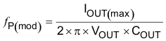
For the example design, the modulator pole is located at 1.5 kHz and the ESR zero is located at 338 kHz.
Next, the designer must select a crossover frequency to determine the bandwidth of the control loop. The crossover frequency must be located at a frequency at least five times higher than the modulator pole. The crossover frequency must also be selected so that the available gain of the error amplifier at the crossover frequency is high enough to allow for proper compensation.
Use Equation 47 to calculate the maximum crossover frequency when the ESR zero is located at a frequency that is higher than the desired crossover frequency which is usually the case for ceramic or low-ESR tantalum capacitors. Aluminum Electrolytic and Tantalum capacitors will typically produce a modulator zero at a low frequency due to their high ESR.
The example application is using a low ESR ceramic capacitor with 10 mΩ of ESR making the zero at 338 kHz.
This value is much higher than typical crossover frequencies so the maximum crossover frequency is calculated using both Equation 43 and Equation 46.
Using Equation 46 results in a minimum crossover frequency of 7.6 kHz and Equation 43 results in a maximum crossover frequency of 45.3 kHz.
A crossover frequency of 45 kHz is arbitrarily selected from this range.
For ceramic capacitors use Equation 43:
For tantalum or aluminum capacitors use Equation 44:
For all cases use Equation 45 and Equation 46:
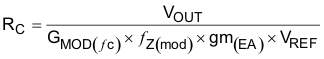
When a crossover frequency, ƒC, is selected, the gain of the modulator at the crossover frequency is calculated. Use Equation 47 to calculate the gain of the modulator at the crossover frequency.
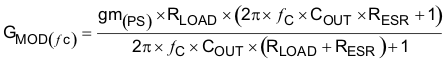
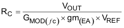
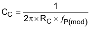
For the example problem, the gain of the modulator at the crossover frequency is 0.542. Next, the compensation components are calculated. A resistor in series with a capacitor is used to create a compensating zero. A capacitor in parallel to these two components forms the compensating pole. However, calculating the values of these components varies depending on if the ESR zero is located above or below the crossover frequency. For ceramic or low-ESR tantalum output capacitors, the zero is usually be located above the crossover frequency. For aluminum electrolytic and tantalum capacitors, the modulator zero is usually located lower in frequency than the crossover frequency. For cases where the modulator zero frequency is higher than the crossover frequency (for example using ceramic capacitors) use Equation 48, Equation 49, and Equation 50 to calculate the RC, CC, and Cƒ values.
For cases where the modulator zero is less than the crossover frequency (Aluminum or Tantalum capacitors), the equations are as follows:
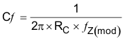
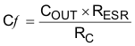
For the example problem, the ESR zero is located at a higher frequency compared to the crossover frequency so Equation 48 through Equation 50 are used to calculate the compensation components. For the example problem, the components are calculated to be: RC = 76.2kΩ, CC = 2710pF, and Cƒ = 6.17pF.
The calculated value of the Cƒ capacitor is not a standard value, so a value of 2700pF is used. A value of 6.8 pF is used for CC. The RC resistor sets the gain of the error amplifier which determines the crossover frequency. The calculated value of the RC resistor is not a standard value, so a value of 76.8 kΩ is used.
9.2.2.11 Power Dissipation Estimate
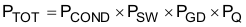
The following formulas show how to estimate the device power dissipation under continuous-conduction mode (CCM) operation. These equations should not be used if the device is working in discontinuous conduction mode (DCM).
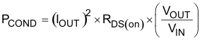
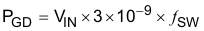
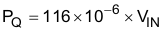
The power dissipation of the device includes conduction loss (PCOND), switching loss (PSW), gate drive loss (PGD) and supply current (PQ).
where
- RDS(on) is the on-resistance of the high-side MOSFET (Ω)
- VOUT is the output voltage (V)
- VIN is the input voltage (V)
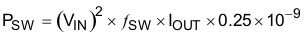
where
- IOUT is the output current (A)
- ƒSW is the switching frequency (Hz)
where
- PTOT s the total device power dissipation (W)
For given TA:
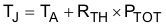
where
- TJ is the junction temperature (°C)
- TA is the ambient temperature (°C)
- RTH is the thermal resistance of the package (°C/W)
For given TJMAX = 150°C:
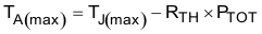
where
- TA(max) is maximum ambient temperature (°C).
- TJ(max) is maximum junction temperature (°C)
Additional power losses occur in the regulator circuit because of the inductor AC and DC losses, the catch diode, and trace resistance that impact the overall efficiency of the regulator.
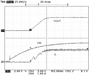
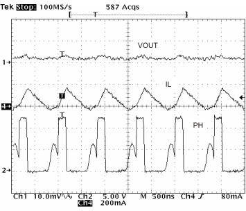
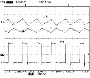
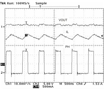
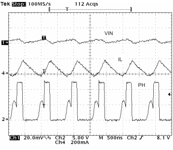
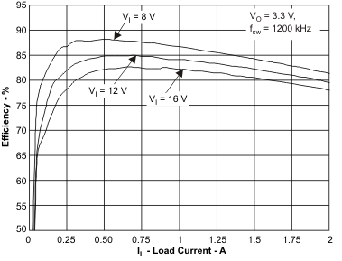
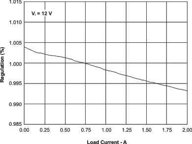
9.2.3 Application Curves