SLVS845G March 2009 – August 2014 TPS54362-Q1
PRODUCTION DATA.
- 1 Features
- 2 Applications
- 3 Description
- 4 Revision History
- 5 Pin Configuration and Functions
- 6 Specifications
-
7 Detailed Description
- 7.1 Overview
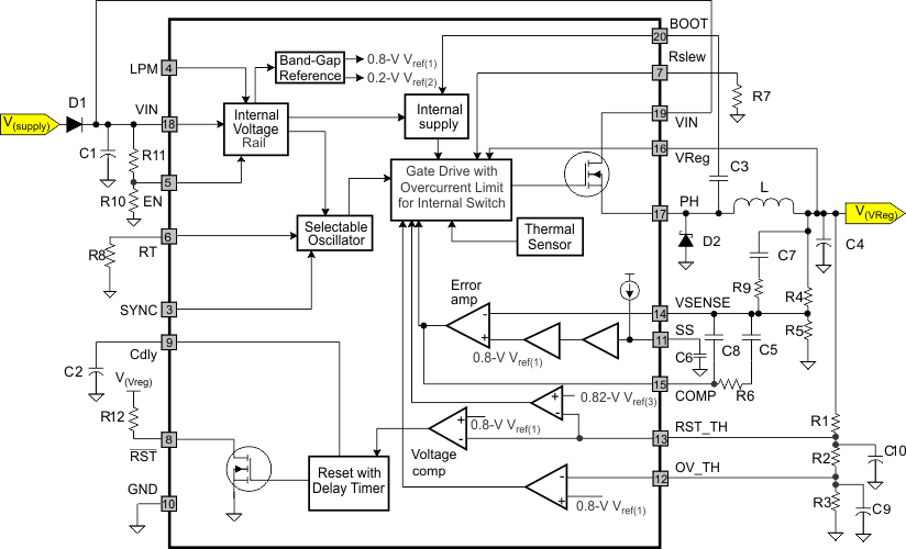
- 7.2 Functional Block Diagram
- 7.3
Feature Description
- 7.3.1 Input Voltage
- 7.3.2 Function Mode
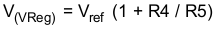
- 7.3.3 Output Voltage V(VReg)
- 7.3.4 Oscillator Frequency (RT)
- 7.3.5 Synchronization (SYNC)
- 7.3.6 Enable or Shutdown (EN)
- 7.3.7 Reset Delay (Cdly)
- 7.3.8 Reset Pin (RST)
- 7.3.9 Boost Capacitor (BOOT)
- 7.3.10 Soft Start (SS)
- 7.3.11 Short-Circuit Protection
- 7.3.12 Overcurrent Protection
- 7.3.13 Slew Rate Control (Rslew)
- 7.3.14 Thermal Shutdown
- 7.3.15 Regulation Voltage (VSENSE)
- 7.3.16 RESET Threshold (RST_TH)
- 7.3.17 Overvoltage Supervisor for V(VReg) (OV_TH)
- 7.3.18 Noise Filter on RST_TH and OV_TH Pins
- 7.3.19 Output Tolerances Based on Modes of Operation
- 7.3.20 Load Regulation and Line Regulation in Hysteretic Mode
- 7.3.21 Internal Undervoltage Lockout (UVLO)
- 7.3.22 Loop-Control Frequency Compensation
- 7.3.23 Bode Plot of Converter Gain
- 7.4 Device Functional Modes
-
8 Application and Implementation
- 8.1 Application Information
- 8.2
Typical Application
- 8.2.1 Design Requirements
- 8.2.2
Detailed Design Procedure
- 8.2.2.1 Selecting the Switching Frequency
- 8.2.2.2 Output Inductor Selection (LO)
- 8.2.2.3 Output Capacitor (CO)
- 8.2.2.4 Flyback Schottky Diode
- 8.2.2.5 Input Capacitor, C(I)
- 8.2.2.6 Output Voltage and Feedback Resistor Selection
- 8.2.2.7 Overvoltage Resistor Selection
- 8.2.2.8 Reset-Threshold Resistor Selection
- 8.2.2.9 Low-Power Mode Threshold
- 8.2.2.10 Undervoltage Threshold for Low-Power Mode and Load-Transient Operation
- 8.2.2.11 Soft-Start Capacitor
- 8.2.2.12 Bootstrap Capacitor Selection
- 8.2.2.13 Guidelines for Compensation Components
- 8.2.2.14 Compensation
- 8.2.3 Application Curves
- 9 Power Supply Recommendations
- 10Layout
- 11Device and Documentation Support
- 12Mechanical, Packaging, and Orderable Information
Package Options
Mechanical Data (Package|Pins)
- PWP|20
Thermal pad, mechanical data (Package|Pins)
- PWP|20
Orderable Information
7 Detailed Description
7.1 Overview
The TPS54362-Q1 device is a 60-V, 3-A DC-DC step-down (buck) converter using a voltage-control-mode scheme. The device features a supervisory function for power-on-reset during system power on. When the output voltage has exceeded the threshold set by the resistor network connected to the RST_TH pin, a delay of 1 ms per nF (based on the capacitor value on the RSTDLY pin) occurs before the release to high of the RST pin. Conversely on power down, once the output voltage falls below the same set threshold, the device pulls RST low only after a de-glitch filter of approximately 20 μs (typical) expires. The implementation of this function prevents the triggering of RST due to fast transient line noise on the output supply.
An overvoltage monitor function limits output voltage to the threshold set by OV_TH. The external resistor network sets both the RST_TH and OV_TH monitoring voltages to be a pre-scale of the output voltage, and the internal bias voltages of the voltage comparators (0.8 V typical) are the basis of the thresholds.
The RST_TH setting is the basis for detection of undervoltage on the output, which invokes low assertion of the RST pin. The OV_TH setting is the basis for detection of overvoltage on the output, which does not invoke low assertion of the RST pin. However, the device commands the internal switch to turn OFF.
In systems where power consumption is critical, implementation of low-power mode reduces the non-switching quiescent current during light load conditions. The system entering discontinuous current mode (DCM) for at least 100 μs determines PFM operation. When the device enters discontinuous mode depends on the selection of external components.
If excessive power dissipation causes invocation of thermal shutdown, the device disables the internal switch, and the regulated output voltage starts to decrease. Depending on the load line, the regulated voltage could decay and the RST_TH threshold may assert the RST output low.
7.3 Feature Description
The TPS54362-Q1 device is a DC-DC converter using a voltage-control-mode scheme with an input voltage feed-forward technique. The device is programmable for a range of output voltages with a wide input-voltage range. The following are details with regard to the pin functionality.
7.3.1 Input Voltage
The VIN pin is the input power source for the TPS54362-Q1 device. This pin requires external protection against voltage levels greater than 60 V and reverse battery. In buck mode, the device draws pulsed input current from this pin, with fast rise and fall times. Therefore, this input line requires a filter capacitor to minimize noise. Additionally, for EMI considerations, the line may also require an input-filter inductor.
7.3.2 Function Mode
| FUNCTION | OPERATING VOLTAGE RANGE | OUTPUT CURRENT CAPABILITY | COMMENTS |
|---|---|---|---|
| Buck | 3.6 V to 48 V | V(VReg) = 0.9 V to 18 V and I(VReg) up to 3 A; however, at higher output power the device requires derating for maximum temperature rating. | Optimum performance: always set V(VIN)-to-V(VReg) ratios such that the minimum required duty cycle pulse (t(ON-Min)) > 150 ns. The minimum off-time is 250 ns for all conditions. |
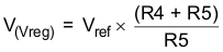
7.3.3 Output Voltage V(VReg)
The converter supplied from battery voltage V(VIN) and the external components (L, C) generate the output voltage, V(VReg). The VSENSE pin senses the output through an external resistor divider and compares it with an internal reference voltage.
Selecting the external resistors according to the relationship in Equation 1 selects the value of the adjustable output voltage between 0.9 V and 18 V in buck mode. Reference designators for the resistors in the following equations refer to the Functional Block Diagram.
where
- R5 and R4 are feedback resistors
- Vref = 0.8 V (typical)
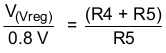
The internal reference voltage has a ±1.5% tolerance. The overall output voltage tolerance depends on the external feedback resistors. To determine the overall output voltage tolerance, use the following relationship:

where
- R4 and R5 are feedback resistors
- Vref = 0.8 V (typical)
The VReg pin also connects internally to a load of 100 Ω, which turns ON in the following conditions:
- During startup conditions, when the device is powered up with no load, or whenever EN is toggled, the internal load connected to the VReg pin turns ON for about 100 µs to charge the bootstrap capacitor to provide gate drive voltage to the switching transistor.
- During normal operating conditions, when the regulated output voltage exceeds the overvoltage threshold (preset by external resisitors R1, R2, and R3), the internal load turns ON, pulling this pin down to bring the regulated output voltage down.
Typically, the output uses a capacitor within the range of 10 μF to 400 μF. This pin must have a filter capacitor with low ESR characteristics in order to minimize output ripple voltage.
7.3.4 Oscillator Frequency (RT)
Oscillator frequency is selectable by means of a resistor placed at the RT pin. The switching frequency (f(SW)) can be set in the range of 200 kHz–2200 kHz. In addition, a clock signal (f(ext)) at the SYNC pin with f(SW) < f(ext) < 2 × f(SW) can externally impose the switching frequency. In this case, the external clock overrides the switching frequency determined by the RT pin, and the external synchronization signal clocks the internal oscillator.
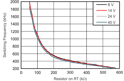 Figure 13. Switching Frequency vs Resistor Value
7.3.5 Synchronization (SYNC)
The SYNC pin is an external input signal to synchronize the switching frequency using an external clock signal. The synchronization input overrides the internally fixed oscillator signal. The synchronization signal must be valid for approximately 2 clock cycles (pulses) before the transition is made for synchronization with the external frequency input. If the external clock input does NOT transition low or high for 32 μS (typical), the system defaults to the internal clock set by the RT pin. The SYNC input clock can have a maximum frequency of 2× the programmed clock frequency up to a maximum value of 2.2 MHz.
7.3.6 Enable or Shutdown (EN)
The enable pin provides electrical on-off control of the regulator. Once the enable pin voltage exceeds the threshold voltage, the regulator starts operation, and the internal soft start begins to ramp. Pulling the enable pin voltage below the threshold voltage stops the regulator from switching, and the internal soft start resets. Connecting the pin to ground or to any voltage less than 0.7 V disables the regulator and activates the shutdown mode. This pin must have an external pullup or pulldown to change the state of the device.
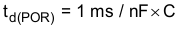
7.3.7 Reset Delay (Cdly)
The reset-delay pin sets the desired delay time to assert the RESET pin high after the supply has exceeded the programmed VReg_RST voltage. One can program the delay in the range of 2.2 ms to 200 ms using capacitors in the range of 2.2 nF to 200 nF. Use Equation 3 to calculate the delay time.
where
- C = capacitance on the Cdly pin
7.3.8 Reset Pin (RST)
The RST pin is an open-drain output. The device asserts the power-on-reset output low until the output voltage exceeds the programmed VReg_RST voltage threshold and the reset delay timer has expired. Additionally, whenever the EN pin is low or open, the device immediately asserts RST low regardless of the output voltage. A reset filter timer prevents reset being invoked because of short negative transients on the output line. If a thermal shutdown occurs due to excessive thermal conditions, the device asserts this pin low when the switching FET is OFF and output falls below the reset threshold.
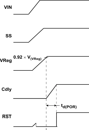 Figure 14. Power-On Condition, Reset Line
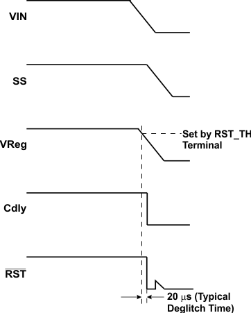 Figure 15. Power-Down Condition, Reset Line
7.3.9 Boost Capacitor (BOOT)
This capacitor provides the gate-drive voltage for the internal MOSFET switch. TI recommends X7R or X5R grade dielectrics because of the stable values over temperature of these dielectrics. Decreasing the value of the boost capacitor for low-Vreg applications, high-frequency applications, or combination applications may be necessary. Increasing the value of the boost capacitor for high-Vreg applications, low-frequency applications, or combination applications may be necessary (for example, 100 nF for 500 kHz at 5 V or 220 nF for 500 kHz at 8 V).
7.3.10 Soft Start (SS)
On power up or after a short-circuit event , TI recommends the following conditions:
- V(VIN) – V(VReg) > 2.5 V
- Load current < 1 A, until RST goes high
C(SS) is 1 nF to 220 nF. If the buck converter starts up with output shorted to ground, the value of C(SS) must be a minimum of 150 nF.
7.3.11 Short-Circuit Protection
The TPS54362-Q1 device features output short-circuit protection. Detection of short-circuit conditions is by monitoring RST_TH, and when the voltage on this node drops below 0.2 V, the switching frequency decreases and the current limit folds back to protect the device. The switching frequency folds back to approximately 25 kHz and the current limit reduces to 30% of the current-limit typical value.
7.3.12 Overcurrent Protection
Implementation of overcurrent protection is by sensing the current through the NMOS switch FET and a comparison of the sensed current to a current reference level representing the overcurrent threshold limit. Sensed current exceeding the overcurrent threshold limit sets the overcurrent indicator to true. The system ignores the overcurrent indicator for the leading edge blanking time at the beginning of each cycle to avoid any turnon-noise glitches.
Setting the overcurrent indicator to true triggers overcurrent protection. The MOSFET turns off for the rest of the cycle after a propagation delay. The name of the overcurrent protection scheme is cycle-by-cycle current limiting. If the sensed current continues to increase during cycle-by-cycle current limiting, the temperature of the device starts rising. At the temperature limit, thermal shutdown (TSD) kicks in and shuts down switching until the device cools sufficiently.
CAUTION
In certain conditions, device damage may occur under a shorted load condition, depending on the supply voltage. The design of the TPS54362-Q1 devices is for protection from damage due to a shorted load condition using a cycle-by-cycle current limit, the short-circuit protection function, and/or the thermal shutdown function.
Short-circuit detection protects the device from damage when encountering a 0-Ω short-circuit condition. However, damage to a device may occur when the shorted load has some resistivity and the output level stays higher than the short-circuit detection level of 0.2 V. In this case, the inductor current increases until the junction temperature of the device hits the thermal shutdown threshold, but damage to the switching FET may occur before thermal shutdown.
This failure only occurs during an output short circuit with some resistivity when the supply voltage is above 18 V.
7.3.13 Slew Rate Control (Rslew)
The Rslew pin controls the switching slew rate of the internal power NMOS. An external resistor with a slew-rate range for rise and fall times as shown in Figure 16 and Figure 17 sets the slew rate. The range of rise time tr = 15 ns to 35 ns, and fall time tf = 15 ns to 200 ns, with Rslew range of 10 kΩ to 50 kΩ (see Figure 16 and Figure 17).
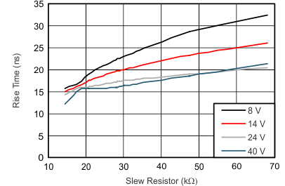 Figure 16. FET Rise Time
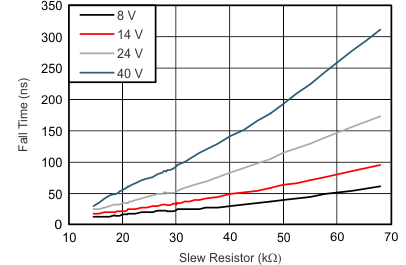 Figure 17. FET Fall Time
7.3.14 Thermal Shutdown
The TPS54362-Q1 device protects itself from overheating with an internal thermal-shutdown circuit. If the junction temperature exceeds the thermal-shutdown trip point, the MOSFET turns off. The device restarts automatically under control of the slow-start circuit when the junction temperature drops below the thermal-shutdown hysteretic trip point. Operating in low-power mode disables the thermal-shutdown sensing circuitry for low current consumption. Asserting RST or V(VReg_UV) low activates thermal-shutdown monitoring.
7.3.15 Regulation Voltage (VSENSE)
Use of the VSENSE pin is for programming the regulated output voltage based on a resistor feedback network monitoring the V(VReg) output voltage. The selected ratio of R4 to R5 sets the VReg voltage.
7.3.16 RESET Threshold (RST_TH)
This pin is programmable for setting the undervoltage threshold level (V(VReg_UV)) for proper regulation in low-power mode and the reset threshold level (V(VReg_RST)) to initiate a reset-output signal. The resistor combination of R1 to R3 programs the threshold for detection of undervoltage. Voltage bias on R2 + R3 sets the reset threshold.
Undervoltage for transient and low-power-mode operation:


Recommended range: 70% to 92% of the regulation voltage
7.3.17 Overvoltage Supervisor for V(VReg) (OV_TH)
This pin is programmable to set the overvoltage monitoring of the regulated output voltage. The resistor combination of R1 to R3 programs the threshold for detection of overvoltage. The bias voltage of R3 sets the OV threshold and the output voltage accuracy in hysteretic mode during transient events.

Recommended range: 106% to 110% of the regulation voltage
7.3.18 Noise Filter on RST_TH and OV_TH Pins
Some noise sensitivity exists on the RST_TH and OV_TH pins, and added capacitance filters this noise. The noise is more pronounced with fast falling edges on the PH pin. So a smaller Rslew resistor (minimum recommended value is 10 kΩ) may require more capacitance on RST_TH and OV_TH. Users should use the smallest capacitance necessary, because larger values increase the loop response time and degrade short-circuit protection and transient response. The 2-μs maximum time constant seen on OV_TH and RST_TH when V(VReg) = 0 V (that is, [R2 + R3] × [C9 + C10] < 2 μs) determines the upper limit. The noise in the RST_TH and OV_TH resistor chain may change with PCB layout or application setup, so there may not be a requirement for the RST_TH and/or OV_TH capacitor in all applications. Users can place the footprint and then populate it only if necessary.
Example:
R1 = 36 kΩ
R2 = 600 Ω
R3 = 6.6 kΩ


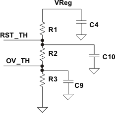 Figure 18. Resistor Network and Noise Filters
Typical values for the RST_TH and OV_TH capacitors are in the 10-pF to 100-pF range for total resistance on the RST_TH-OV_TH divider of < 200 kΩ.
7.3.19 Output Tolerances Based on Modes of Operation
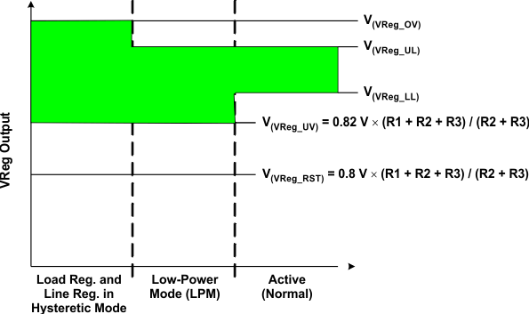 Figure 19. Modes of Operation
Table 1. Values for Threshold Voltages in Each Mode of Operation
| MODE OF OPERATION | V(VReg) - LOWER LIMIT | V(VReg) – UPPER LIMIT | COMMENTS |
|---|---|---|---|
| Hysteretic mode | 0.82 V × (R1 + R2 + R3) / (R2 + R3) | 0.8 V × (R1 + R2 + R3) / (R3) | Minimum to maximum ripple on output |
| Low-power mode | 0.82 V × (R1 + R2 + R3) / (R2 + R3) | V(VReg) + V(VReg-tol) | Minimum to maximum ripple on output |
| Active (normal) | V(VReg) – V(VReg-tol) | V(VReg) + V(VReg-tol) | Minimum to maximum ripple on output |
Table 2. Values for Threshold Voltages of Voltage Supervisors
| SUPERVISOR THRESHOLDS | V(VReg) - TYPICAL VALUE | TOLERANCE | COMMENTS |
|---|---|---|---|
| Overvoltage | 0.8 V × (R1 + R2 + R3) / (R3) | ± (V(VRef-tol) + (R1 + R2 / [R1 + R2 + R3]) × (R1-tol + R2-tol + R3-tol) | Overvoltage threshold setting |
| Reset | 0.8 V × (R1 + R2 + R3) / (R2 + R3) | ± (V(VRef-tol) + (R1 / [R1 + R2 + R3]) × (R1-tol + R2-tol + R3-tol) |
Reset threshold setting |
7.3.20 Load Regulation and Line Regulation in Hysteretic Mode
This mode of operation is when a load or line transient step occurs in the application. The converter goes into a hysteretic mode of operation until the error amplifier stabilizes and controls the output regulation to a tighter output tolerance. During the load step, V(VReg_OV) sets the regulator upper threshold and the V(VReg_UV) limit sets the lower threshold.
The converter enters this mode of operation during load- or line-transient events if the main control loop cannot respond to regulate within the specified tolerances. The regulator exits this mode once the main control loop responds.
7.3.21 Internal Undervoltage Lockout (UVLO)
On power up, the internal band-gap and bias currents attaining stability, which is typically at V(VIN) = 3.4 V (minimum), enables the IC. On power down, disabling the internal circuitry occurs at V(VIN) = 2.6 V (maximum).
7.3.22 Loop-Control Frequency Compensation
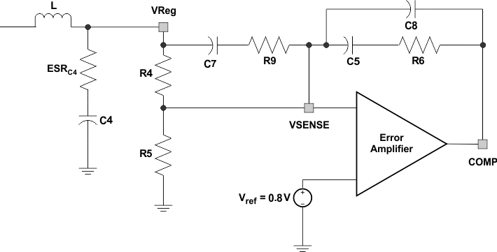 Figure 20. Type III Compensation
7.3.22.1 Type III Compensation
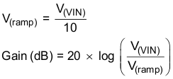
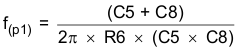
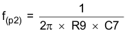
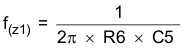
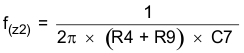
f(c) = f(SW) × 0.1 (unity-gain frequency is the name of the cutoff frequency when the gain is 1).
f(c) is typically 1/5 to 1/10 of the switching frequency, and is typically greater than five times the double-pole frequency of the LC filter.
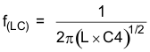
Equation 9 and Equation 10 derive the modulator break frequencies as a function of the output LC filter. The LC output filter gives a double pole, which has a –180 degree phase shift.
The ESR of the output capacitor C gives a zero that has a 90° phase shift.
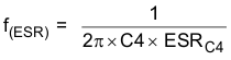
The V(VIN) / V(ramp) modulator gain is about 10 for 8 V < VIN < 50 V. V(ramp) is fixed at 1 V for V(VIN) < 8 V and at 5 V for V(VIN) > 48 V.
Note that the V(VIN) / V(ramp) gain (A(mod)) is not precise and has a tolerance of about 20%.

7.3.23 Bode Plot of Converter Gain
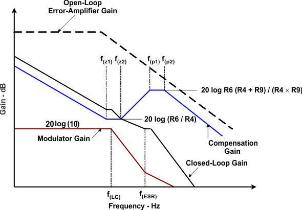 Figure 21. Bode Plot of Converter Gain
7.4 Device Functional Modes
7.4.1 Low-Power Mode (LPM)
The TPS54362-Q1 device automatically enters low-power mode once the regulation goes into discontinuous mode. The internal control circuitry for any transition from low-power mode to high-power mode occurs within 5 μs (typical). In low-power mode, the converter operates as a hysteretic controller with the threshold limits set by V(VReg_UV) = 0.82 × (R1 + R2 +R3 / (R2 + R3) for the lower limit and approximately V(VReg) for the upper limit. To ensure tight regulation in the low-power mode, set the R2 and R3 values accordingly.
The device operates with both automatic and digitally controlled low-power mode. The digital low-power mode can override the automatic low-power mode function by applying the appropriate signal on the LPM pin. The device goes into active or normal mode for at least 100 μs on the tripping of RST_TH or VREG_UV. Operating in active mode or normal mode enables all blocks, including the OV function.
Being in LPM disables the OV function.
Active or normal mode: When the device is in DCM with LPM = High or in CCM with LPM = High or Low
LPM: When part is in DCM with LPM = Low
| Automatic and Digital | |
| LPM high: | LPM high forces the device to normal mode at fixed frequency, even at light load current (the device does pulse skipping to keep output voltage in regulation at light loads). |
| LPM low or open: | The device automatically changes between normal and low-power mode depending on load current. |
7.4.2 Buck-Mode Low-Power-Mode Operation
When operating in low-power mode (buck regulator) with the output shorted to ground, the device asserts a reset. The thermal-shutdown and current-limiting circuitry activates to protect the device.
Low-power-mode operation begins once the converter enters the discontinuous mode of operation.
7.4.3 External LPM Operation
The low-power mode (LPM) is active-low; if there is an open on this pin the IC enters the low-power mode (internal pulldown).
To allow low-power mode operation, the load current must be low with the LPM pin set to ground.
To inhibit low-power mode, the microcontroller must drive the pin high, and the converter must not be in discontinuous mode of operation.
The device can only power up in LPM or DCM if V(VReg) < 5.5 V and V(VIN) – V(VReg) > 2.5 V.
In active mode. the device powers up when V(VIN) > 3.6 V (minimum).
NOTE
Being in LPM prevents enabling of the OV_TH circuit.
Active or normal mode: When the device is in CCM or DCM with LPM = High
LPM: When the device is in DCM with LPM = Low