SLVS845G March 2009 – August 2014 TPS54362-Q1
PRODUCTION DATA.
- 1 Features
- 2 Applications
- 3 Description
- 4 Revision History
- 5 Pin Configuration and Functions
- 6 Specifications
-
7 Detailed Description
- 7.1 Overview
- 7.2 Functional Block Diagram
- 7.3
Feature Description
- 7.3.1 Input Voltage
- 7.3.2 Function Mode
- 7.3.3 Output Voltage V(VReg)
- 7.3.4 Oscillator Frequency (RT)
- 7.3.5 Synchronization (SYNC)
- 7.3.6 Enable or Shutdown (EN)
- 7.3.7 Reset Delay (Cdly)
- 7.3.8 Reset Pin (RST)
- 7.3.9 Boost Capacitor (BOOT)
- 7.3.10 Soft Start (SS)
- 7.3.11 Short-Circuit Protection
- 7.3.12 Overcurrent Protection
- 7.3.13 Slew Rate Control (Rslew)
- 7.3.14 Thermal Shutdown
- 7.3.15 Regulation Voltage (VSENSE)
- 7.3.16 RESET Threshold (RST_TH)
- 7.3.17 Overvoltage Supervisor for V(VReg) (OV_TH)
- 7.3.18 Noise Filter on RST_TH and OV_TH Pins
- 7.3.19 Output Tolerances Based on Modes of Operation
- 7.3.20 Load Regulation and Line Regulation in Hysteretic Mode
- 7.3.21 Internal Undervoltage Lockout (UVLO)
- 7.3.22 Loop-Control Frequency Compensation
- 7.3.23 Bode Plot of Converter Gain
- 7.4 Device Functional Modes
-
8 Application and Implementation
- 8.1 Application Information
- 8.2
Typical Application
- 8.2.1 Design Requirements
- 8.2.2
Detailed Design Procedure
- 8.2.2.1 Selecting the Switching Frequency
- 8.2.2.2 Output Inductor Selection (LO)
- 8.2.2.3 Output Capacitor (CO)
- 8.2.2.4 Flyback Schottky Diode
- 8.2.2.5 Input Capacitor, C(I)
- 8.2.2.6 Output Voltage and Feedback Resistor Selection
- 8.2.2.7 Overvoltage Resistor Selection
- 8.2.2.8 Reset-Threshold Resistor Selection
- 8.2.2.9 Low-Power Mode Threshold
- 8.2.2.10 Undervoltage Threshold for Low-Power Mode and Load-Transient Operation
- 8.2.2.11 Soft-Start Capacitor
- 8.2.2.12 Bootstrap Capacitor Selection
- 8.2.2.13 Guidelines for Compensation Components
- 8.2.2.14 Compensation
- 8.2.3 Application Curves
- 9 Power Supply Recommendations
- 10Layout
- 11Device and Documentation Support
- 12Mechanical, Packaging, and Orderable Information
Package Options
Mechanical Data (Package|Pins)
- PWP|20
Thermal pad, mechanical data (Package|Pins)
- PWP|20
Orderable Information
6 Specifications
6.1 Absolute Maximum Ratings
over operating free-air temperature (unless otherwise noted) (1)(1) Stresses beyond those listed under Absolute Maximum Ratings may cause permanent damage to the device. These are stress ratings only, which do not imply functional operation of the device at these or any other conditions beyond those indicated under Recommended Operating Conditions. Exposure to absolute-maximum-rated conditions for extended periods may affect device reliability.
6.2 Handling Ratings
| MIN | MAX | UNIT | ||||
|---|---|---|---|---|---|---|
| Tstg | Storage temperature range | –55 | 165 | °C | ||
| V(ESD) | Electrostatic discharge | Human-body model (HBM), per AEC Q100-002(1) | –2 | 2 | kV | |
| Charged-device model (CDM), per AEC Q100-011 | –750 | 750 | V | |||
(1) AEC Q100-002 indicates HBM stressing is done in accordance with the ANSI/ESDA/JEDEC JS-001 specification.
6.3 Recommended Operating Conditions
over operating free-air temperature (unless otherwise noted)| MIN | MAX | UNIT | ||
|---|---|---|---|---|
| VI | Unregulated buck supply input voltage (VIN, EN) | 3.6 | 48 | V |
| V(VReg) | Regulator voltage range | 0.9 | 18 | V |
| Power up in low-power mode (LPM) or discontinuous mode (DCM) | 0.9 | 5.5 | ||
| Logic level inputs (RST, VSENSE, OV_TH, RST_TH, SYNC, RT) | 0 | 5.25 | V | |
| Logic level inputs (SS, Cdly, COMP) | 0 | 6.5 | V | |
| TJ | Operating junction temperature range(1) | –40 | 150 | °C |
(1) This assumes TA = TJ – Power dissipation × RθJA (junction-to-ambient).
6.4 Thermal Information
| THERMAL METRIC(1) | TPS54362-Q1 | UNIT | |
|---|---|---|---|
| PWP | |||
| 20 PINS | |||
| RθJA | Junction-to-ambient thermal resistance | 43.8 | °C/W |
| RθJC(top) | Junction-to-case (top) thermal resistance | 21.4 | |
| RθJB | Junction-to-board thermal resistance | 18.5 | |
| ψJT | Junction-to-top characterization parameter | 0.5 | |
| ψJB | Junction-to-board characterization parameter | 18.3 | |
| RθJC(bot) | Junction-to-case (bottom) thermal resistance | 1.2 | |
(1) For more information about traditional and new thermal metrics, see the Semiconductor and IC Package Thermal Metrics application report, SPRA953.
6.5 Electrical Characteristics
V(VIN) = 7 V to 48 V, V(EN) = V(VIN), TJ = –40°C to 150°C (unless otherwise noted)| PARAMETER | TEST CONDITIONS | MIN | TYP | MAX | UNIT | TEST(1) | ||
|---|---|---|---|---|---|---|---|---|
| INPUT POWER SUPPLY | ||||||||
| V(VIN) | Supply voltage on VIN pin | Normal mode–buck mode after initial start-up | 3.6 | 48 | V | Info | ||
| Low-power mode | Falling threshold (LPM disabled) | 8 | V | |||||
| Rising threshold (LPM activated) | 8.5 | |||||||
| High-voltage threshold (LPM disabled) | 25 | 27 | 30 | |||||
| I(q-Normal) | Quiescent current, normal mode | Open-loop test – maximum duty cycle V(VIN) = 7 V to 48 V |
5 | 10 | mA | PT | ||
| I(q-LPM) | Quiescent current; low-power mode | I(VReg) < 1 mA, V(VIN) = 12 V, TA = 25°C | 65 | 75 | μA | PT | ||
| I(VReg) < 1 mA, V(VIN) = 12 V, –40 < TJ < 150°C | 75 | |||||||
| I(VReg) < 1 mA, V(VIN) = 24 V, TA = 25°C | 85 | |||||||
| I(VReg) < 1 mA, V(VIN) = 24 V, –40 < TJ < 150°C | 85 | |||||||
| I(SD) | Shutdown | V(EN) = 0 V, device is OFF, TA = –40°C to 125°C, V(VIN) = 24 V |
10 | μA | PT | |||
| V(EN) = 0 V, device is OFF, TA = 25°C, V(VIN) = 12 V | 1 | 4 | ||||||
| TRANSITION TIMES (LOW-POWER AND NORMAL MODES) | ||||||||
| td(1) | Transition delay from normal mode to low-power mode | V(VIN) = 12 V, V(VReg) = 5 V, I(VReg) = 1 A to 1 mA | 100 | μs | CT | |||
| td(2) | Transition delay from low-power mode to normal mode | V(VIN) = 12 V, V(VReg) = 5 V, I(VReg) = 1 mA to 1 A | 5 | μs | CT | |||
| SWITCH-MODE SUPPLY (VReg) | ||||||||
| V(VReg) | Regulator output | V(VSENSE) = 0.8-V reference | 0.9 | 18 | V | Info | ||
| V(VSENSE) | Feedback voltage | V(VReg) = 0.9 V to 18 V, V(VIN) = 7 V to 48 V | 0.788 | 0.8 | 0.812 | V | CT | |
| rDS(on) | Internal switch resistance | Measured across VIN and PH, I(VReg) = 500 mA | 500 | mΩ | PT | |||
| I(CL) | Switch current limit, cycle-by-cycle | V(VIN) = 12 V | 4 | 6 | 8 | A | Info | |
| t(ON-Min) | Duty-cycle pulse duration (ON) | 50 | 100 | 150 | ns | Info | ||
| t(OFF-Min) | Duty-cycle pulse duration (OFF) | 100 | 200 | 250 | ns | Info | ||
| f(SW) | Switch-mode frequency | Set using external resistor on RT pin | 0.2 | 2.2 | MHz | PT | ||
| Accuracy of f(SW) | –10% | 10% | PT | |||||
| I(Sink) | Sink current in start-up condition | V(OV_TH) = 0 V, V(VReg) = 10 V | 1 | mA | Info | |||
| I(Limit) | Sink-current limit | 0 V < V(OV_TH) < 0.8 V, V(VReg) = 10 V | 80 | mA | Info | |||
| ENABLE (EN) | ||||||||
| VIL | Low input threshold | 0.7 | V | PT | ||||
| VIH | High input threshold | 1.7 | V | PT | ||||
| Ilkg | Leakage into EN pin | A-revision, V(EN) = 60 V | 100 | 135 | μA | PT | ||
| A-revision,, V(EN) = 12 V | 8 | 15 | ||||||
| B-revision, V(EN) = 60 V | 10 | |||||||
| B-revision, V(EN) = 12 V | 2 | |||||||
| RESET DELAY (Cdly) | ||||||||
| IO | External capacitor charge current | V(EN) = high | 1.4 | 2 | 2.6 | μA | PT | |
| VThreshold | Switching threshold | Output voltage in regulation | 2 | V | PT | |||
| LOW-POWER MODE (LPM) | ||||||||
| VIL | Low input threshold | V(VIN) = 12 V | 0.7 | V | PT | |||
| VIH | High input threshold | V(VIN) = 12 V | 1.7 | V | PT | |||
| Ilkg | Leakage into LPM pin | V(LPM) = 5 V | 65 | 95 | μA | PT | ||
| RESET OUTPUT (RST) | ||||||||
| V(RST_TH) | Reset threshold for RST_TH pin | 0.768 | 0.832 | V | PT | |||
| SOFT START (SS) | ||||||||
| I(SS) | Soft-start source current | 40 | 50 | 60 | μA | PT | ||
| SYNCHRONIZATION (SYNC)(2) | ||||||||
| VIL(SYNC) | Low input threshold | 0.7 | V | PT | ||||
| VIH(SYNC) | High input threshold | 1.7 | V | PT | ||||
| Ilkg | Leakage | SYNC = 5 V | 65 | 95 | μA | PT | ||
| Duty(min) | Minimum duty cycle | 30% | CT | |||||
| Duty(miax) | Maximum duty cycle | 70% | CT | |||||
| Rslew | ||||||||
| I(Rslew) | Output current | Rslew = 50 kΩ | 20 | μA | CT | |||
| Rslew = 10 kΩ | 100 | |||||||
| OVERVOLTAGE SUPERVISORS (OV_TH) | ||||||||
| V(OV_TH) | Threshold for OV_TH pin during OV | Internal switch is OFF. | 0.768 | 0.832 | V | PT | ||
| Internal pulldown current on OV_TH pin | OV_TH = 1 V, V(VReg) = 5 V | 70 | mA | |||||
| THERMAL SHUTDOWN | ||||||||
| T(SD) | Thermal shutdown junction temperature | 175 | °C | CT | ||||
| T(HYS) | Temperature hysteresis | 30 | °C | CT | ||||
(1) PT = Production tested; CT = Characterization tested only, not production tested; Info = User information only, not production tested
(2) The SYNC input clock can have a maximum frequency of 2× the programmed clock frequency up to a maximum value of 1.1 MHz.
6.6 Timing Requirements
V(VIN) = 7 V to 48 V, V(EN) = V(VIN), TJ = –40°C to 150°C (unless otherwise noted)| MIN | NOM | MAX | UNIT | TEST(1) | |||
|---|---|---|---|---|---|---|---|
| SYNCHRONIZATION (SYNC)(2) | |||||||
| t(trans-ItoE) | Internal clock to external clock | External clock = 1 MHz, V(VIN) = 12 V, V(VReg) = 5 V |
2.5 | μs | Info | ||
| f(SYNC) | Input clock | V(VIN) = 12 V, V(VReg) = 5 V, f(sw) < f(ext) < 2 × f(sw) |
180 | 2200 | kHz | CT | |
| RESET OUTPUT (RST) | |||||||
| td(POR) | POR delay timer | C2 = 4.7 nF | 3.6 | 7 | ms | PT | |
| td(RSTdly) | Filter time | 10 | 20 | 35 | μs | PT | |
6.7 Switching Characteristics
V(VIN) = 7 V to 48 V, V(EN) = V(VIN), TJ = –40°C to 150°C (unless otherwise noted)| PARAMETER | TEST CONDITIONS | MIN | TYP | MAX | UNIT | TEST(1) | |
|---|---|---|---|---|---|---|---|
| SYNCHRONIZATION (SYNC)(2) | |||||||
| t(trans-EtoI) | External clock to internal clock | Remove external clock, V(VIN) = 12 V, V(VReg) = 5 V | 32 | μs | Info | ||
6.8 Typical Characteristics
6.8.1 Efficiency Data of Power Supply
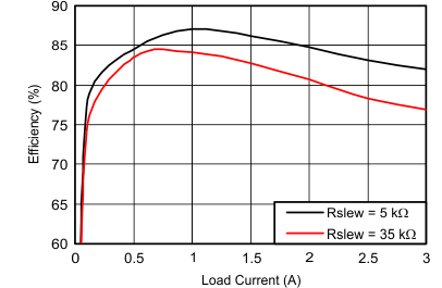
| V(VIN) = 12 V | V(VReg) = 5 V | f(SW) = 500 kHz |
| L = 22 µH | C4 (output) = 100 µF | TA = 25ºC |
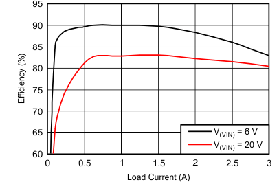
| V(VReg) = 5 V | f(SW) = 500 kHz | L = 22 µH |
| C4 (output) = 100 µF | Rslew = 5 kΩ | TA = 25ºC |
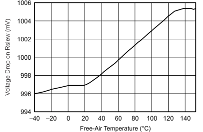
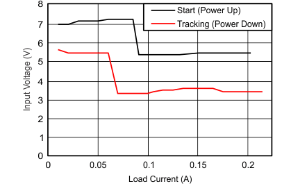
6.8.2 Output Voltage Dropout
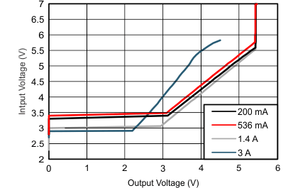
| V(VReg) = 5 V | f(SW) = 500 kHz |
| V(VReg) = 5 V | TA = 25ºC |
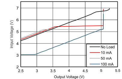
| V(VReg) = 5 V | f(SW) = 500 kHz |
NOTE
Tracking: The input voltage at which the output voltage drops approximately –0.7 V of the regulated voltage or for low input voltages (tracking function) over the load range.
Start: The input voltage required to achieve 5-V regulation on power up with the stated load currents.
6.8.3 Quiescent and Standby Current
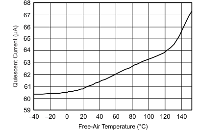
| V(VIN) = 12 V |
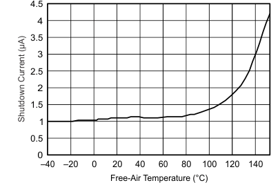
| V(VIN) = 12 V |
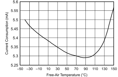
| EN = High | V(VIN) = 12 V |
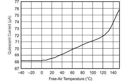
| V(VIN) = 24 V |
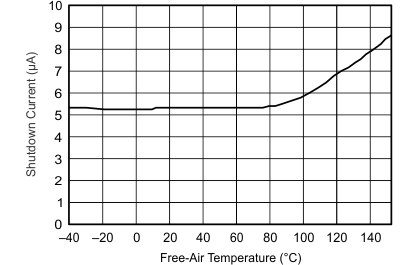
| V(VIN) = 24 V |
6.8.4 Reference Voltages
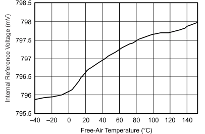
| V(VIN) = 12 V |