SLVSDQ8B October 2016 – June 2021 TPS54388C-Q1
PRODUCTION DATA
- 1 Features
- 2 Applications
- 3 Description
- 4 Revision History
- 5 Pin Configuration and Functions
- 6 Specifications
-
7 Detailed Description
- 7.1 Overview
- 7.2 Functional Block Diagram
- 7.3 Feature Description
- 7.4
Device Functional Modes
- 7.4.1 Adjusting the Output Voltage
- 7.4.2 Enable Functionality and Adjusting Undervoltage Lockout
- 7.4.3 Slow-Start or Tracking Pin
- 7.4.4 Sequencing
- 7.4.5 Constant Switching Frequency and Timing Resistor (RT/CLK Pin)
- 7.4.6 Overcurrent Protection
- 7.4.7 Frequency Shift
- 7.4.8 Reverse Overcurrent Protection
- 7.4.9 Synchronize Using the RT/CLK Pin
- 7.4.10 Power Good (PWRGD Pin)
- 7.4.11 Overvoltage Transient Protection
- 7.4.12 Thermal Shutdown
- 7.4.13 Small-Signal Model for Loop Response
- 7.4.14 Simple Small-Signal Model for Peak-Current-Mode Control
- 7.4.15 Small-Signal Model for Frequency Compensation
-
8 Application and Implementation
- 8.1 Application Information
- 8.2
Typical Application
- 8.2.1 Design Requirements
- 8.2.2
Detailed Design Procedure
- 8.2.2.1 Selecting the Switching Frequency
- 8.2.2.2 Output Inductor Selection
- 8.2.2.3 Output Capacitor
- 8.2.2.4 Input Capacitor
- 8.2.2.5 Slow-Start Capacitor
- 8.2.2.6 Bootstrap Capacitor Selection
- 8.2.2.7 Output-Voltage and Feedback-Resistor Selection
- 8.2.2.8 Compensation
- 8.2.2.9 Power-Dissipation Estimate
- 8.2.3 Application Curves
- 9 Power Supply Recommendations
- 10Layout
- 11Device and Documentation Support
- 12Mechanical, Packaging, and Orderable Information
Package Options
Mechanical Data (Package|Pins)
- RTE|16
Thermal pad, mechanical data (Package|Pins)
- RTE|16
Orderable Information
8.2.2.2 Output Inductor Selection
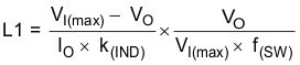
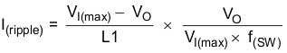
The inductor selected works for the entire TPS54388C-Q1 input-voltage range. To calculate the value of the output inductor, use Equation 22. The k(IND) coefficient represents the amount of inductor ripple current relative to the maximum output current. The output capacitor filters the inductor ripple current. Therefore, choosing high inductor ripple currents impacts the selection of the output capacitor, because the output capacitor must have a ripple-current rating equal to or greater than the inductor ripple current. In general, the inductor ripple value is at the discretion of the designer; however, k(IND) is normally from 0.1 to 0.3 for the majority of applications.
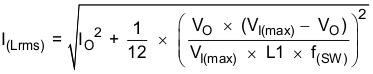
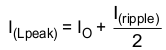
For this design example, use k(IND) = 0.3, and the inductor value calculates to be 1.36 μH. For this design, choose the nearest standard value of 1.5 μH. For the output-filter inductor, it is important not to exceed the rms-current and saturation-current ratings. Find the rms and peak inductor current using Equation 24 and Equation 25.
For this design, the rms inductor current is 3.01 A and the peak inductor current is 3.72 A. The chosen inductor is a Coilcraft XLA4020-152ME_ or equivalent. It has a saturation current rating 0f 9.6 A and an RMS current rating of 7.5 A.
The current flowing through the inductor is the inductor ripple current plus the output current. During power up, faults, or transient load conditions, the inductor current can increase above the calculated peak inductor current level calculated previously. In transient conditions, the inductor current can increase up to the switch-current limit of the device. For this reason, the most conservative approach is to specify an inductor with a saturation current rating equal to or greater than the switch-current limit rather than the peak inductor current.