SLVSDQ8B October 2016 – June 2021 TPS54388C-Q1
PRODUCTION DATA
- 1 Features
- 2 Applications
- 3 Description
- 4 Revision History
- 5 Pin Configuration and Functions
- 6 Specifications
-
7 Detailed Description
- 7.1 Overview
- 7.2 Functional Block Diagram
- 7.3 Feature Description
- 7.4
Device Functional Modes
- 7.4.1 Adjusting the Output Voltage
- 7.4.2 Enable Functionality and Adjusting Undervoltage Lockout
- 7.4.3 Slow-Start or Tracking Pin
- 7.4.4 Sequencing
- 7.4.5 Constant Switching Frequency and Timing Resistor (RT/CLK Pin)
- 7.4.6 Overcurrent Protection
- 7.4.7 Frequency Shift
- 7.4.8 Reverse Overcurrent Protection
- 7.4.9 Synchronize Using the RT/CLK Pin
- 7.4.10 Power Good (PWRGD Pin)
- 7.4.11 Overvoltage Transient Protection
- 7.4.12 Thermal Shutdown
- 7.4.13 Small-Signal Model for Loop Response
- 7.4.14 Simple Small-Signal Model for Peak-Current-Mode Control
- 7.4.15 Small-Signal Model for Frequency Compensation
-
8 Application and Implementation
- 8.1 Application Information
- 8.2
Typical Application
- 8.2.1 Design Requirements
- 8.2.2
Detailed Design Procedure
- 8.2.2.1 Selecting the Switching Frequency
- 8.2.2.2 Output Inductor Selection
- 8.2.2.3 Output Capacitor
- 8.2.2.4 Input Capacitor
- 8.2.2.5 Slow-Start Capacitor
- 8.2.2.6 Bootstrap Capacitor Selection
- 8.2.2.7 Output-Voltage and Feedback-Resistor Selection
- 8.2.2.8 Compensation
- 8.2.2.9 Power-Dissipation Estimate
- 8.2.3 Application Curves
- 9 Power Supply Recommendations
- 10Layout
- 11Device and Documentation Support
- 12Mechanical, Packaging, and Orderable Information
Package Options
Mechanical Data (Package|Pins)
- RTE|16
Thermal pad, mechanical data (Package|Pins)
- RTE|16
Orderable Information
8.2.2.4 Input Capacitor
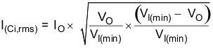
The TPS54388C-Q1 device requires a high-quality ceramic, type X5R or X7R, input decoupling capacitor with at least 4.7 μF of effective capacitance, and in some applications a bulk capacitance. The effective capacitance includes any dc bias effects. The voltage rating of the input capacitor must be greater than the maximum input voltage. The capacitor must also have a ripple-current rating greater than the maximum input-current ripple of the TPS54388C-Q1 device. Calculate the input ripple current using Equation 30.
The value of a ceramic capacitor varies significantly over temperature and the amount of dc bias applied to the capacitor. Minimize the capacitance variations due to temperature by selecting a dielectric material that is stable over temperature. X5R and X7R ceramic dielectrics are the usual selection for power regulator capacitors because they have a high capacitance-to-volume ratio and are fairly stable over temperature. The output-capacitor selection must also take dc bias into account. The capacitance value of a capacitor decreases as the dc bias across that capacitor increases.
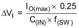
This example design requires a ceramic capacitor with at least a 10-V voltage rating to support the maximum input voltage. For this example, the selection is one 10-μF 10-V and one 0.1-μF 10-V capacitor in parallel. The input capacitance value determines the input ripple voltage of the regulator. Calculate the input voltage ripple using Equation 31. Using the design example values, IO(max) = 3 A, C(IN) = 10 μF, and f(SW) = 1 MHz, yields an input voltage ripple of 76 mV and an rms input ripple current of 1.47 A.