SLVSDQ8B October 2016 – June 2021 TPS54388C-Q1
PRODUCTION DATA
- 1 Features
- 2 Applications
- 3 Description
- 4 Revision History
- 5 Pin Configuration and Functions
- 6 Specifications
-
7 Detailed Description
- 7.1 Overview
- 7.2 Functional Block Diagram
- 7.3 Feature Description
- 7.4
Device Functional Modes
- 7.4.1 Adjusting the Output Voltage
- 7.4.2 Enable Functionality and Adjusting Undervoltage Lockout
- 7.4.3 Slow-Start or Tracking Pin
- 7.4.4 Sequencing
- 7.4.5 Constant Switching Frequency and Timing Resistor (RT/CLK Pin)
- 7.4.6 Overcurrent Protection
- 7.4.7 Frequency Shift
- 7.4.8 Reverse Overcurrent Protection
- 7.4.9 Synchronize Using the RT/CLK Pin
- 7.4.10 Power Good (PWRGD Pin)
- 7.4.11 Overvoltage Transient Protection
- 7.4.12 Thermal Shutdown
- 7.4.13 Small-Signal Model for Loop Response
- 7.4.14 Simple Small-Signal Model for Peak-Current-Mode Control
- 7.4.15 Small-Signal Model for Frequency Compensation
-
8 Application and Implementation
- 8.1 Application Information
- 8.2
Typical Application
- 8.2.1 Design Requirements
- 8.2.2
Detailed Design Procedure
- 8.2.2.1 Selecting the Switching Frequency
- 8.2.2.2 Output Inductor Selection
- 8.2.2.3 Output Capacitor
- 8.2.2.4 Input Capacitor
- 8.2.2.5 Slow-Start Capacitor
- 8.2.2.6 Bootstrap Capacitor Selection
- 8.2.2.7 Output-Voltage and Feedback-Resistor Selection
- 8.2.2.8 Compensation
- 8.2.2.9 Power-Dissipation Estimate
- 8.2.3 Application Curves
- 9 Power Supply Recommendations
- 10Layout
- 11Device and Documentation Support
- 12Mechanical, Packaging, and Orderable Information
Package Options
Mechanical Data (Package|Pins)
- RTE|16
Thermal pad, mechanical data (Package|Pins)
- RTE|16
Orderable Information
8.2.2.9 Power-Dissipation Estimate
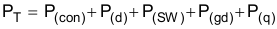
The following formulas show how to estimate the IC power dissipation under continuous-conduction mode (CCM) operation. The power dissipation of the IC (PT) includes conduction loss (P(con)), dead-time loss (P(d)), switching loss (P(SW)), gate-drive loss (P(gd)) and supply-current loss (P(q)).
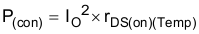
where
- IO is the output current (A)
- rDS(on)(Temp) is the on-resistance of the high-side MOSFET at a given temperature (Ω)
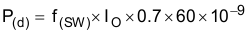
where
- f(SW) is the switching frequency (Hz)
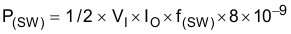
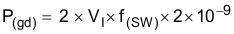
where
- VI is the input voltage (V)
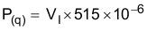
Therefore:
For a given TA, use Equation 48 to calculate the junction temperature.
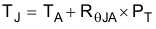
where
- TJ is the junction temperature (°C)
- TA is the ambient temperature (°C)
- RθJA is the thermal resistance of the package (°C/W)
- PT is the total device power dissipation (W)
For a given TJ(max) = 150°C, use Equation 49 to calculate the maximum ambient temperature.
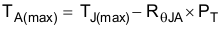
where
- TJ(max) is maximum junction temperature (°C)
- TA(max) is maximum ambient temperature (°C)
Additional power losses occur in the regulator circuit because of the inductor ac and dc losses and trace resistance that impact the overall efficiency of the regulator.