SLVS834B July   2008  – June 2019 TPS5450-Q1

PRODUCTION DATA.  

  1. Features
  2. Applications
  3. Description
    1.     Device Images
      1.      Simplified Schematic and Efficiency Curve
  4. Revision History
  5. Pin Configuration and Functions
    1.     Pin Functions
  6. Specifications
    1. 6.1 Absolute Maximum Ratings
    2. 6.2 Recommended Operating Conditions
    3. 6.3 Thermal Information
    4. 6.4 Dissipation Ratings
    5. 6.5 Electrical Characteristics
    6. 6.6 Typical Characteristics
  7. Detailed Description
    1. 7.1 Overview
    2. 7.2 Functional Block Diagram
    3. 7.3 Feature Description
      1. 7.3.1  Oscillator Frequency
      2. 7.3.2  Voltage Reference
      3. 7.3.3  Enable (ENA) and Internal Slow Start
      4. 7.3.4  Undervoltage Lockout (UVLO)
      5. 7.3.5  Output Feedback (VSENSE) and Internal Compensation
      6. 7.3.6  Voltage Feedforward
      7. 7.3.7  Pulse-Width-Modulation (PWM) Control
      8. 7.3.8  Overcurrent Limiting
      9. 7.3.9  Overvoltage Protection
      10. 7.3.10 Thermal Shutdown
  8. Application Information
    1. 8.1 Application Information
    2. 8.2 Typical Application
      1. 8.2.1 Design Requirements
      2. 8.2.2 Detailed Design Procedure
        1. 8.2.2.1  Custom Design With WEBENCH® Tools
        2. 8.2.2.2  Boost Capacitor (BOOT)
        3. 8.2.2.3  Switching Frequency
        4. 8.2.2.4  Input Capacitors
        5. 8.2.2.5  Output Filter Components
          1. 8.2.2.5.1 Inductor Selection
          2. 8.2.2.5.2 Capacitor Selection
        6. 8.2.2.6  Output Voltage Setpoint
        7. 8.2.2.7  Boot Capacitor
        8. 8.2.2.8  Catch Diode
        9. 8.2.2.9  Output Voltage Limitations
        10. 8.2.2.10 Internal Compensation Network
      3. 8.2.3 Application Curves
  9. Layout
    1. 9.1 Layout Guidelines
    2. 9.2 Layout Examples
    3. 9.3 Thermal Calculations
  10. 10Device and Documentation Support
    1. 10.1 Device Support
      1. 10.1.1 Third-Party Products Disclaimer
    2. 10.2 Development Support
      1. 10.2.1 Custom Design With WEBENCH® Tools
    3. 10.3 Receiving Notification of Documentation Updates
    4. 10.4 Community Resources
    5. 10.5 Trademarks
    6. 10.6 Electrostatic Discharge Caution
    7. 10.7 Glossary
  11. 11Mechanical, Packaging, and Orderable Information

Package Options

Mechanical Data (Package|Pins)
Thermal pad, mechanical data (Package|Pins)
Orderable Information

Typical Characteristics

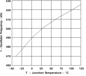
TPS5450-Q1 f_jt_lvs632.gif
Figure 1. Oscillator Frequency vs Junction Temperature
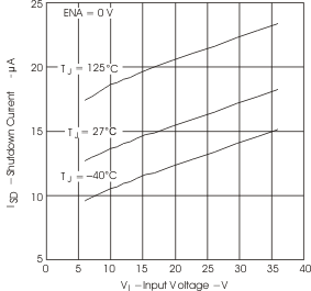
TPS5450-Q1 isd_vi_lvs632.gif
Figure 3. Shutdown Quiescent Currentvsinput Voltage
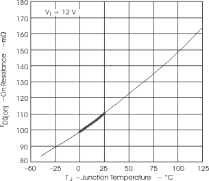
TPS5450-Q1 rdson_jt_lvs632.gif
Figure 5. On-Resistance vs Junction Temperature
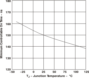
TPS5450-Q1 mcot_jt_lvs632.gif
Figure 7. Minimum Controllable On-Time vs Junction Temperature
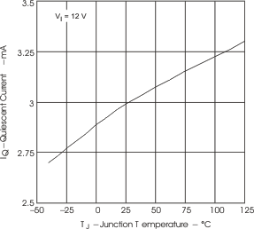
TPS5450-Q1 iq_jt_lvs632.gif
Figure 2. Non-Switching Quiescent Current vs Junction Temperature
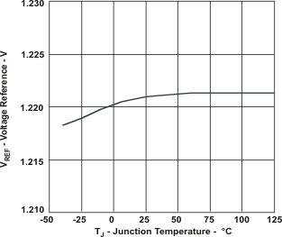
TPS5450-Q1 vref_jt_lvs632.gif
Figure 4. Voltage Reference vs Junction Temperature
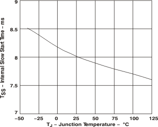
TPS5450-Q1 tss_jt_lvs632.gif
Figure 6. Internal Slow Start Time vs Junction Temperature
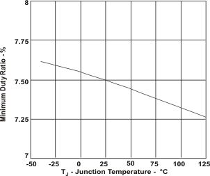
TPS5450-Q1 mdr_jt_lvs632.gif
Figure 8. Minimum Controllable Duty Ratio vs Junction Temperature