SNVSBB1D March 2020 – July 2021 TPS548A28
PRODUCTION DATA
- 1 Features
- 2 Applications
- 3 Description
- 4 Revision History
- 5 Pin Configuration and Functions
- 6 Specifications
-
7 Detailed Description
- 7.1 Overview
- 7.2 Functional Block Diagram
- 7.3
Feature Description
- 7.3.1 Internal VCC LDO And Using External Bias On VCC Pin
- 7.3.2 Enable
- 7.3.3 Output Voltage Setting
- 7.3.4 Internal Fixed Soft Start and External Adjustable Soft Start
- 7.3.5 External REFIN For Output Voltage Tracking
- 7.3.6 Frequency and Operation Mode Selection
- 7.3.7 D-CAP3 Control
- 7.3.8 Low-side FET Zero-Crossing
- 7.3.9 Current Sense and Positive Overcurrent Protection
- 7.3.10 Low-side FET Negative Current Limit
- 7.3.11 Power Good
- 7.3.12 Overvoltage and Undervoltage Protection
- 7.3.13 Out-Of-Bounds (OOB) Operation
- 7.3.14 Output Voltage Discharge
- 7.3.15 UVLO Protection
- 7.3.16 Thermal Shutdown
- 7.4 Device Functional Modes
-
8 Application and Implementation
- 8.1 Application Information
- 8.2
Typical Application
- 8.2.1 Design Requirements
- 8.2.2
Detailed Design Procedure
- 8.2.2.1 Output Voltage Setting Point
- 8.2.2.2 Choose the Switching Frequency and the Operation Mode
- 8.2.2.3 Choose the Inductor
- 8.2.2.4 Set the Current Limit (TRIP)
- 8.2.2.5 Choose the Output Capacitor
- 8.2.2.6 Choose the Input Capacitors (CIN)
- 8.2.2.7 Soft Start Capacitor (SS/REFIN Pin)
- 8.2.2.8 EN Pin Resistor Divider
- 8.2.2.9 VCC Bypass Capacitor
- 8.2.2.10 BOOT Capacitor
- 8.2.2.11 PGOOD Pullup Resistor
- 8.2.3 Application Curves
- 9 Power Supply Recommendations
- 10Layout
- 11Device and Documentation Support
- 12Mechanical, Packaging, and Orderable Information
Package Options
Mechanical Data (Package|Pins)
- RWW|21
Thermal pad, mechanical data (Package|Pins)
Orderable Information
8.2.2.2 Choose the Switching Frequency and the Operation Mode
The switching frequency and operation mode are configured by the resistor on MODE pin. Select one of three switching frequencies: 600 kHz, 800 kHz, or 1 MHz. Refer to Table 7-1 for the relationship between the switching frequency, operation mode and RMODE.
Switching frequency selection is a tradeoff between higher efficiency and smaller system solution size. Lower switching frequency yields higher overall efficiency but relatively bigger external components. Higher switching frequencies cause additional switching losses which impact efficiency and thermal performance. For this design, a 243-kΩ resistor is chosen for MODE pin to set the switching frequency to 0.8 MHz and set operation mode as skip mode.
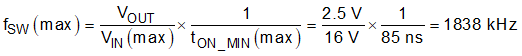
When selecting the switching frequency of a buck converter, the minimum on-time and minimum off-time must be considered. Equation 8 calculates the maximum fSW before being limited by the minimum on-time. When hitting the minimum on-time limits of a converter with D-CAP3 control, the effective switching frequency will change to keep the output voltage regulated. This calculation ignores resistive drops in the converter to give a worst case estimation.
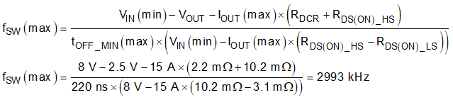
Equation 8 calculates the maximum fSW before being limited by the minimum off-time. When hitting the minimum off-time limits of a converter with D-CAP3 control, the operating duty cycle will max out and the output voltage will begin to drop with the input voltage. This equation requires the DC resistance of the inductor, RDCR, selected in the following step so this preliminary calculation assumes a resistance of 2.2 mΩ. If operating near the maximum fSW limited by the minimum off-time, the variation in resistance across temperature must be considered when using Equation 9. The selected fSW of 800 kHz is below the two calculated maximum values.