SLUSC70D March 2016 – July 2017 TPS548D22
PRODUCTION DATA.
- 1 Features
- 2 Applications
- 3 Description
- 4 Revision History
- 5 Pin Configuration and Functions
- 6 Specifications
-
7 Detailed Description
- 7.1 Overview
- 7.2 Functional Block Diagram
- 7.3 Feature Description
- 7.4 Device Functional Modes
- 7.5 Programming
-
8 Application and Implementation
- 8.1 Application Information
- 8.2
Typical Applications
- 8.2.1 TPS548D22 1.5-V to 16-V Input, 1-V Output, 40-A Converter
- 8.2.2 Design Requirements
- 8.2.3
Design Procedure
- 8.2.3.1 Switching Frequency Selection
- 8.2.3.2 Inductor Selection
- 8.2.3.3 Output Capacitor Selection
- 8.2.3.4 Input Capacitor Selection
- 8.2.3.5 Bootstrap Capacitor Selection
- 8.2.3.6 BP Pin
- 8.2.3.7 R-C Snubber and VIN Pin High-Frequency Bypass
- 8.2.3.8 Optimize Reference Voltage (VSEL)
- 8.2.3.9 MODE Pin Selection
- 8.2.3.10 Overcurrent Limit Design.
- 8.2.4 Application Curves
- 9 Power Supply Recommendations
- 10Layout
- 11Device and Documentation Support
- 12Mechanical, Packaging, and Orderable Information
Package Options
Mechanical Data (Package|Pins)
- RVF|40
Thermal pad, mechanical data (Package|Pins)
- RVF|40
Orderable Information
7.5.1.3.1 Application Workaround to Support 4-ms and 8-ms SS Settings
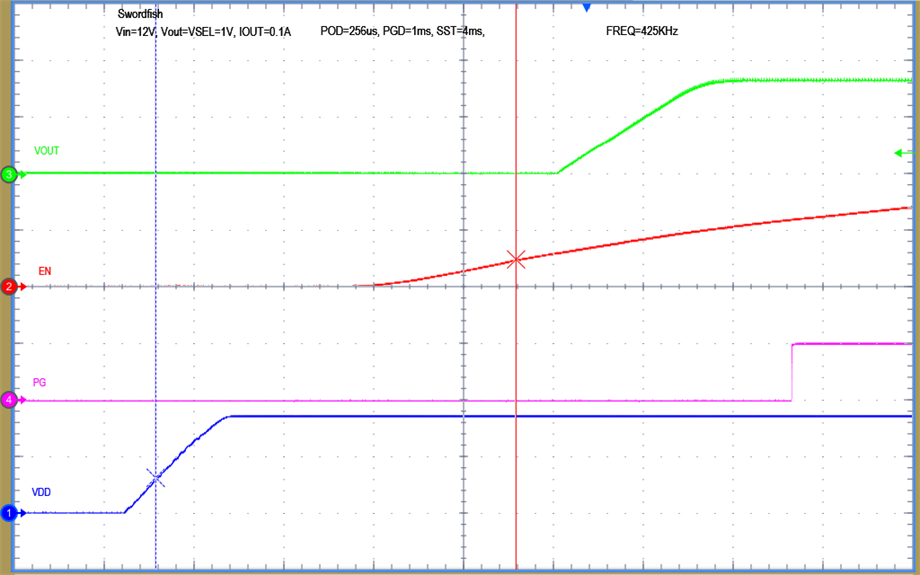
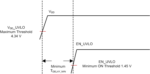
In order to properly design for 4-ms and 8-ms SS settings, additional application consideration is needed. The recommended application workaround to support the 4-ms and 8-ms soft-start settings is to ensure sufficient time delay between the VDD and EN_UVLO signals. The minimum delay between the rising maximum VDD_UVLO level and the minimum turnon threshold of EN_UVLO is at least TDELAY_MIN.
where
- K = 9 ms/V for SS setting of 4 ms
- K = 18 ms/V for SS setting of 8 ms
- VREF is the internal reference voltage programmed by VSEL pin strap
For example, if SS setting is 4 ms and VREF = 1 V, program the minimum delay at least 9 ms; if SS setting is 8 ms, the minimum delay should be programmed at least 18 ms. See Figure 16 and Figure 17 for detailed timing requirement.
 Figure 16. Proper Sequencing of VDD and EN_UVLO to Support the use of 4-ms SS Setting
 Figure 17. Minimum Delay Between VDD and EN_UVLO to Support the use of 4-ms and 8-ms SS settings
The workaround/consideration described previously is not required for SS settings of 1 ms and 2 ms.