SLUSCI9A August 2016 – September 2017 TPS549D22
PRODUCTION DATA.
- 1 Features
- 2 Applications
- 3 Description
- 4 Revision History
- 5 Pin Configuration and Functions
- 6 Specifications
-
7 Detailed Description
- 7.1 Overview
- 7.2 Functional Block Diagram
- 7.3 Feature Description
- 7.4 Device Functional Modes
- 7.5
Programming
- 7.5.1 Programmable Pin-Strap Settings
- 7.5.2 Programmable Analog Configurations
- 7.5.3 PMBus Programming
- 7.5.4
Register Maps
- 7.5.4.1 OPERATION Register (address = 1h)
- 7.5.4.2 ON_OFF_CONFIG Register (address = 2h)
- 7.5.4.3 CLEAR FAULTS (address = 3h)
- 7.5.4.4 WRITE PROTECT (address = 10h)
- 7.5.4.5 STORE_DEFAULT_ALL (address = 11h)
- 7.5.4.6 RESTORE_DEFAULT_ALL (address = 12h)
- 7.5.4.7 CAPABILITY (address = 19h)
- 7.5.4.8 VOUT_MODE (address = 20h)
- 7.5.4.9 VOUT_COMMAND (address = 21h)
- 7.5.4.10 VOUT_MARGIN_HIGH (address = 25h)
- 7.5.4.11 VOUT_MARGIN_LOW (address = 26h)
- 7.5.4.12 STATUS_BYTE (address = 78h)
- 7.5.4.13 STATUS_WORD (High Byte) (address = 79h)
- 7.5.4.14 STATUS_VOUT (address = 7Ah)
- 7.5.4.15 STATUS_IOUT (address = 7Bh)
- 7.5.4.16 STATUS_CML (address = 7Eh)
- 7.5.4.17 MFR_SPECIFIC_00 (address = D0h)
- 7.5.4.18 MFR_SPECIFIC_01 (address = D1h)
- 7.5.4.19 MFR_SPECIFIC_02 (address = D2h)
- 7.5.4.20 MFR_SPECIFIC_03 (address = D3h)
- 7.5.4.21 MFR_SPECIFIC_04 (address = D4h)
- 7.5.4.22 MFR_SPECIFIC_06 (address = D6h)
- 7.5.4.23 MFR_SPECIFIC_07 (address = D7h)
- 7.5.4.24 MFR_SPECIFIC_44 (address = FCh)
-
8 Application and Implementation
- 8.1 Application Information
- 8.2
Typical Application: TPS549D22 1.5-V to 16-V Input, 1-V Output, 40-A Converter
- 8.2.1 Design Requirements
- 8.2.2
Detailed Design Procedure
- 8.2.2.1 Custom Design With WEBENCH® Tools
- 8.2.2.2 Switching Frequency Selection
- 8.2.2.3 Inductor Selection
- 8.2.2.4 Output Capacitor Selection
- 8.2.2.5 Input Capacitor Selection
- 8.2.2.6 Bootstrap Capacitor Selection
- 8.2.2.7 BP Pin
- 8.2.2.8 R-C Snubber and VIN Pin High-Frequency Bypass
- 8.2.2.9 Optimize Reference Voltage (VSEL)
- 8.2.2.10 MODE Pin Selection
- 8.2.2.11 ADDR Pin Selection
- 8.2.2.12 Overcurrent Limit Design
- 8.2.3 Application Curves
- 9 Power Supply Recommendations
- 10Layout
- 11Device and Documentation Support
- 12Mechanical, Packaging, and Orderable Information
- 13Package Option Addendum
Package Options
Refer to the PDF data sheet for device specific package drawings
Mechanical Data (Package|Pins)
- RVF|40
Thermal pad, mechanical data (Package|Pins)
- RVF|40
Orderable Information
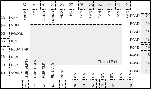
5 Pin Configuration and Functions
RVF Package
40-Pin LQFN-CLIP With Thermal Pad
Top View

Pin Functions
| PIN | I/O/P(1) | DESCRIPTION | |
|---|---|---|---|
| NAME | NO. | ||
| AGND | 30 | G | Ground pin for internal analog circuits. |
| BOOT | 5 | P | Supply rail for high-side gate driver (boot terminal). Connect boot capacitor from this pin to SW node. Internally connected to BP via bootstrap PMOS switch. |
| BP | 31 | O | LDO output |
| DRGND | 29 | P | Internal gate driver return. |
| EN_UVLO | 4 | I | Enable pin that can turn on the DC/DC switching converter. Use also to program the required PVIN UVLO when PVIN and VDD are connected together. |
| ADDR | 32 | I | Program device address and SKIP or FCCM mode. |
| ILIM | 36 | I/O | Program overcurrent limit by connecting a resistor to ground. |
| MODE | 34 | I | Mode selection pin. Select the control mode (DCAP3 or DCAP), and soft-start timing selection. |
| NC | 27 | No connect. | |
| PGND | 13, 14, 15, 16, 17, 18, 19, 20 | P | Power ground of internal FETs. |
| PGOOD | 35 | O | Open drain power good status signal. |
| PMB_CLK | 3 | I | Clock input for the PMBus interface. |
| PMB_DATA | 2 | I/O | Data I/O for the PMBus interface. |
| PVIN | 21, 22, 23, 24, 25, 26 | P | Power supply input for integrated power MOSFET pair. |
| RSN | 38 | I | Inverting input of the differential remote sense amplifier. |
| RSP | 39 | I | Non-inverting input of the differential remote sense amplifier. |
| RESV_TRK | 37 | I | Do not connect. |
| SMB_ALRT# | 1 | O | Alert output for the PMBus interface. |
| SW | 6 , 7, 8, 9, 10, 11, 12 | I/O | Output switching terminal of power converter. Connect the pins to the output inductor. |
| VDD | 28 | P | Controller power supply input. |
| VOSNS | 40 | I | Output voltage monitor input pin. |
| VSEL | 33 | I | Program the initial start-up and or reference voltage without feedback resistor dividers (from 0.6 V to 1.2 V in 50-mV increments). |
(1) I = input, O = output, G = GND