SLVSEQ0A May   2019  – March 2020 TPS54A24

PRODUCTION DATA.  

  1. Features
  2. Applications
    1.     Simplified Schematic
  3. Description
    1.     Efficiency (VIN = 12 V, fSW = 500 kHz)
  4. Revision History
  5. Pin Configuration and Functions
    1.     Pin Functions
  6. Specifications
    1. 6.1 Absolute Maximum Ratings
    2. 6.2 ESD Ratings
    3. 6.3 Recommended Operating Conditions
    4. 6.4 Thermal Information
    5. 6.5 Electrical Characteristics
    6. 6.6 Timing Requirements
    7. 6.7 Switching Characteristics
    8. 6.8 Typical Characteristics
  7. Detailed Description
    1. 7.1 Overview
    2. 7.2 Functional Block Diagram
    3. 7.3 Feature Description
      1. 7.3.1  Fixed Frequency PWM Control
      2. 7.3.2  Continuous Conduction Mode Operation (CCM)
      3. 7.3.3  VIN Pins and VIN UVLO
      4. 7.3.4  Voltage Reference and Adjusting the Output Voltage
      5. 7.3.5  Error Amplifier
      6. 7.3.6  Enable and Adjustable UVLO
      7. 7.3.7  Soft Start and Tracking
      8. 7.3.8  Safe Start-Up Into Prebiased Outputs
      9. 7.3.9  Power Good
      10. 7.3.10 Sequencing (SS/TRK)
      11. 7.3.11 Adjustable Switching Frequency (RT Mode)
      12. 7.3.12 Synchronization (CLK Mode)
      13. 7.3.13 Bootstrap Voltage and 100% Duty Cycle Operation (BOOT)
      14. 7.3.14 Output Overvoltage Protection (OVP)
      15. 7.3.15 Overcurrent Protection
        1. 7.3.15.1 High-Side MOSFET Overcurrent Protection
        2. 7.3.15.2 Low-Side MOSFET Overcurrent Protection
    4. 7.4 Device Functional Modes
  8. Application and Implementation
    1. 8.1 Application Information
    2. 8.2 Typical Application
      1. 8.2.1 Design Requirements
      2. 8.2.2 Detailed Design Procedure
        1. 8.2.2.1  Custom Design With WEBENCH® Tools
        2. 8.2.2.2  Switching Frequency
        3. 8.2.2.3  Output Inductor Selection
        4. 8.2.2.4  Output Capacitor
        5. 8.2.2.5  Input Capacitor
        6. 8.2.2.6  Output Voltage Resistors Selection
        7. 8.2.2.7  Soft-Start Capacitor Selection
        8. 8.2.2.8  Undervoltage Lockout Setpoint
        9. 8.2.2.9  Bootstrap Capacitor Selection
        10. 8.2.2.10 PGOOD Pullup Resistor
        11. 8.2.2.11 Compensation
      3. 8.2.3 Application Curves
  9. Power Supply Recommendations
  10. 10Layout
    1. 10.1 Layout Guidelines
    2. 10.2 Layout Example
  11. 11Device and Documentation Support
    1. 11.1 Device Support
      1. 11.1.1 Development Support
        1. 11.1.1.1 Custom Design With WEBENCH® Tools
    2. 11.2 Receiving Notification of Documentation Updates
    3. 11.3 Community Resources
    4. 11.4 Trademarks
    5. 11.5 Electrostatic Discharge Caution
    6. 11.6 Glossary
  12. 12Mechanical, Packaging, and Orderable Information

Package Options

Mechanical Data (Package|Pins)
Thermal pad, mechanical data (Package|Pins)
Orderable Information

Typical Characteristics

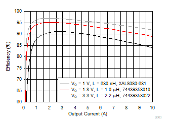
TPS54A24 D003-efficiency-5Vin-500kHz-slvseq0.gif
VIN = 5 V fSW = 500 kHz
Figure 1. Efficiency with 5-V Input and 500-kHz Switching Frequency
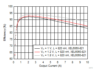
TPS54A24 D010-efficiency-5V-XEL6060.gif
VIN = 5 V fSW = 500 kHz
Figure 3. Efficiency With 5-V Input, 500-kHz Switching Frequency and 6.36-mm × 6.56-mm Inductor
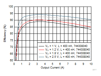
TPS54A24 D011-efficiency-5V-1MHz.gif
VIN = 5 V fSW = 1 MHz
Figure 5. Efficiency With 5-V Input and 1 MHz Switching Frequency
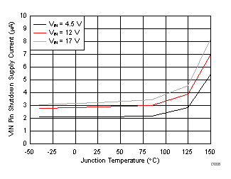
TPS54A24 D006_slvsdc9.gif
V(EN) = 0.4 V
Figure 7. VIN Pin Shutdown Current vs Junction Temperature
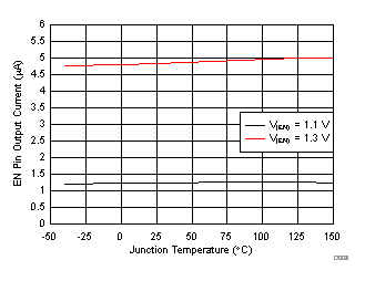
TPS54A24 D008_slvsdc9.gif
Figure 9. EN Pin Current vs Junction Temperature
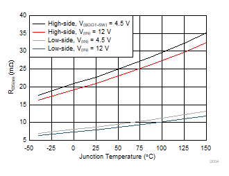
TPS54A24 D004-Rdson-vs-temp.gif
Figure 11. MOSFET RDS(on) vs Junction Temperature
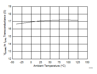
TPS54A24 D009_gmps.gif
Figure 13. V(COMP) to I(SW) Transconductance vs Ambient Temperature
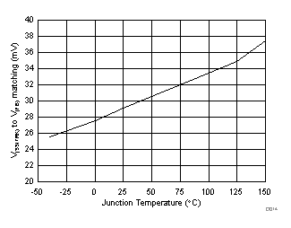
TPS54A24 D014_slvsdc9.gif
V(SS/TRK) = 0.4 V
Figure 15. SS/TRK to FB Offset vs Junction Temperature
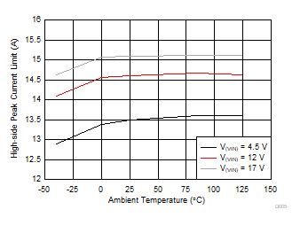
TPS54A24 D005-HSOC-vs-temp.gif
L = 1.0 µH
Figure 17. High-side Peak Current Limit vs Ambient Temperature
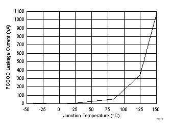
TPS54A24 D017_slvsdc9.gif
V(FB) = 0.6 V V(PGOOD) = 5 V
Figure 19. PGOOD Leakage Current vs Junction Temperature
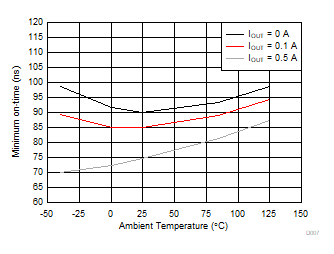
TPS54A24 D007-tonmin-vs-ta.gif
V(VIN) = 12 V L = 1.0 µH
Figure 21. Minimum on-time vs Ambient Temperature
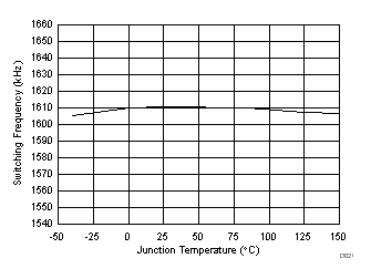
TPS54A24 D021_slvsdc9.gif
R(RT/CLK) = 30.1 kΩ
Figure 23. Switching Frequency vs Junction Temperature (1600 kHz)
TPS54A24 D024_slvsdc9.gif
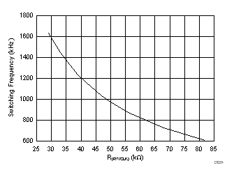
Figure 25. Switching Frequency vs RT/CLK Resistor (High Range)
TPS54A24 D008-efficiency-5v-9v.gif
VIN = 12 V fSW = 500 kHz
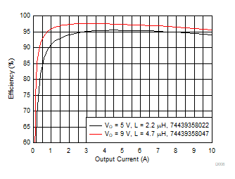
Figure 2. Efficiency With 5-V and 9-V Output
TPS54A24 D009-efficiency-12V-XEL6060.gif
VIN = 12 V fSW = 500 kHz
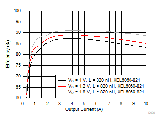
Figure 4. Efficiency With 12-V Input, 500-kHz Switching Frequency and 6.36 mm × 6.56 mm Inductor
TPS54A24 D005_slvsdc9.gif
V(EN) = 5 V V(FB) = 0.8 V
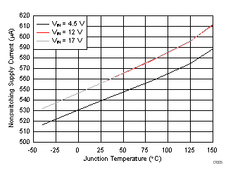
Figure 6. VIN Pin Nonswitching Supply Current vs Junction Temperature
TPS54A24 D007_slvsdc9.gif
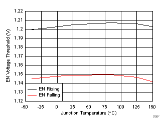
Figure 8. EN Pin Voltage Threshold vs Junction Temperature
TPS54A24 D009_slvsdc9.gif
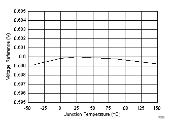
Figure 10. Regulated FB Voltage vs Junction Temperature
TPS54A24 D011_slvsdc9.gif
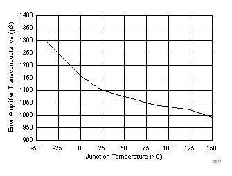
Figure 12. Error Amplifier Transconductance vs Junction Temperature
TPS54A24 D013_slvsdc9.gif
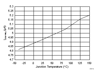
Figure 14. SS/TRK Current vs Junction Temperature
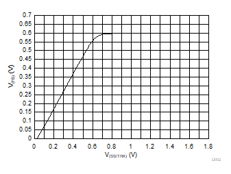
TPS54A24 D002-Vfb-vs-Vss.gif
Figure 16. FB voltage vs SS/TRK Voltage
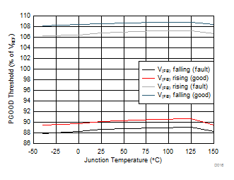
TPS54A24 D016_slvsdc9.gif
Figure 18. PGOOD Thresholds vs Junction Temperature
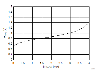
TPS54A24 D006-minvin-validpg.gif
TJ = 25 °C V(PGOOD) < 0.5 V
Figure 20. Minimum Input Voltage for Valid PGOOD Output vs PGOOD Current
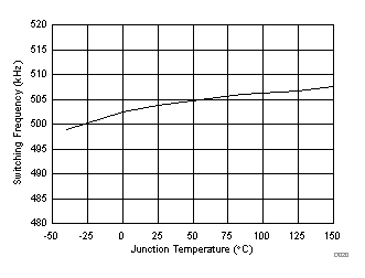
TPS54A24 D020_slvsdc9.gif
R(RT/CLK) = 100 kΩ
Figure 22. Switching Frequency vs Junction Temperature (500 kHz)
TPS54A24 D023_slvsdc9.gif
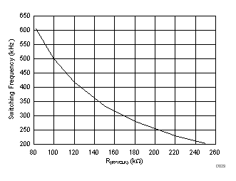
Figure 24. Switching Frequency vs RT/CLK Resistor (Low Range)