SLVSFQ8A December 2020 – December 2021 TPS552882-Q1
PRODUCTION DATA
- 1 Features
- 2 Applications
- 3 Description
- 4 Revision History
- 5 Pin Configuration and Functions
- 6 Specifications
-
7 Detailed Description
- 7.1 Overview
- 7.2 Functional Block Diagram
- 7.3
Feature Description
- 7.3.1 VCC Power Supply
- 7.3.2 Operation Mode Setting
- 7.3.3 Input Undervoltage Lockout
- 7.3.4 Enable and Programmable UVLO
- 7.3.5 Soft Start
- 7.3.6 Shutdown
- 7.3.7 Switching Frequency
- 7.3.8 Switching Frequency Dithering
- 7.3.9 Inductor Current Limit
- 7.3.10 Internal Charge Path
- 7.3.11 Output Voltage Setting
- 7.3.12 Output Current Indication and Cable Voltage Drop Compensation
- 7.3.13 Integrated Gate Drivers
- 7.3.14 Output Current Limit
- 7.3.15 Overvoltage Protection
- 7.3.16 Output Short Circuit Protection
- 7.3.17 Thermal Shutdown
- 7.4 Device Functional Modes
- 8 Application and Implementation
- 9 Power Supply Recommendations
- 10Layout
- 11Device and Documentation Support
- 12Mechanical, Packaging, and Orderable Information
Package Options
Mechanical Data (Package|Pins)
- RPM|26
Thermal pad, mechanical data (Package|Pins)
- RPM|26
Orderable Information
7.3.12 Output Current Indication and Cable Voltage Drop Compensation
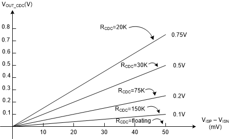
The TPS55288 outputs a voltage at the CDC pin proportional to the sensed voltage across a output current sensing resistor between the ISP pin and the ISN pin. Equation 7 shows the exact voltage at the CDC pin related to the sensed output current.

To compensate the voltage drop across a cable from the terminal of the USB port to its powered device, the TPS552882-Q1 can lift its output voltage in proportion to the load current by placing a resistor between the CDC pin and AGND pin.
When using external output voltage feedback on the TPS552882-Q1, the output voltage rises in proportional to the current sourcing from the CDC pin through the resistor at the CDC pin. It is recommended to use 100-kΩ resistance for the up resistor of the resistor divider. Equation 8 shows the output voltage rise versus the sensed output current, resistance at the CDC pin and the up resistor of the output voltage feedback resistor divider.

where
- RFB_UP is the up resistor of the resistor divider between the output and the FB/INT pin
- RCDC is the resistor at the CDC pin
When RFB_UP is 100 kΩ, the output voltage rise versus the sensed output current and the resistor at the CDC pin is shown in Figure 7-6
 Figure 7-6 Output Voltage Rise versus Output
Current