SLVSBD4E May 2012 – September 2021 TPS55340
PRODUCTION DATA
- 1 Features
- 2 Applications
- 3 Description
- 4 Revision History
- 5 Pin Configuration and Functions
- 6 Specifications
- 7 Detailed Description
-
8 Application and Implementation
- 8.1 Application Information
- 8.2
Typical Applications
- 8.2.1
Boost Converter
- 8.2.1.1 Design Requirements
- 8.2.1.2
Detailed Design Procedure
- 8.2.1.2.1 Custom Design with WEBENCH Tools
- 8.2.1.2.2 Selecting the Switching Frequency (R4)
- 8.2.1.2.3 Determining the Duty Cycle
- 8.2.1.2.4 Selecting the Inductor (L1)
- 8.2.1.2.5 Computing the Maximum Output Current
- 8.2.1.2.6 Selecting the Output Capacitors (C8, C9, C10)
- 8.2.1.2.7 Selecting the Input Capacitors (C2, C7)
- 8.2.1.2.8 Setting Output Voltage (R1, R2)
- 8.2.1.2.9 Setting the Soft-start Time (C7)
- 8.2.1.2.10 Selecting the Schottky Diode (D1)
- 8.2.1.2.11 Compensating the Control Loop (R3, C4, C5)
- 8.2.1.3 Application Curves
- 8.2.2
SEPIC Converter
- 8.2.2.1 Design Requirements
- 8.2.2.2
Detailed Design Procedure
- 8.2.2.2.1 Selecting the Switching Frequency (R4)
- 8.2.2.2.2 Duty Cycle
- 8.2.2.2.3 Selecting the Inductor (L1)
- 8.2.2.2.4 Calculating the Maximum Output Current
- 8.2.2.2.5 Selecting the Output Capacitors (C8, C9, C10)
- 8.2.2.2.6 Selecting the Series Capacitor (C6)
- 8.2.2.2.7 Selecting the Input Capacitor (C2, C7)
- 8.2.2.2.8 Selecting the Schottky Diode (D1)
- 8.2.2.2.9 Setting the Output Voltage (R1, R2)
- 8.2.2.2.10 Setting the Soft-start Time (C3)
- 8.2.2.2.11 MOSFET Rating Considerations
- 8.2.2.2.12 Compensating the Control Loop (R3, C4)
- 8.2.2.3 Application Curves
- 8.2.1
Boost Converter
- 9 Power Supply Recommendations
- 10Layout
- 11Device and Documentation Support
- 12Mechanical, Packaging, and Orderable Information
Package Options
Mechanical Data (Package|Pins)
Thermal pad, mechanical data (Package|Pins)
Orderable Information
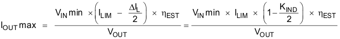
8.2.1.2.5 Computing the Maximum Output Current
The overcurrent limit for the integrated power MOSFET limits the maximum input current and thus the maximum input power for a given input voltage. Maximum output power is less than maximum input power due to power conversion losses. Therefore, the current limit setting, input voltage, output voltage, and efficiency can all change maximum current output (IOUTmax). The current limit clamps the peak inductor current; therefore, the ripple has to be subtracted to derive maximum dc current. Decreasing the KIND or designing for a higher efficiency will increase the maximum output current. This can be evaluated with the chosen inductance or the chosen KIND. This should be evaluated with the minimum input voltage and minimum peak current limit (ILIM) of 5.25 A.
In this design with a 5-V input boosted to a 24-V output and a 10-μH inductor with an assumed Schottky forward voltage of 0.5 V and estimated efficiency of 85%, the maximum output current is 871 mA. With the 12-V input and increased estimated efficiency of 90%, the maximum output current increases to 2.13 A. This circuit was evaluated to its maximum output currents with both the minimum and maximum input voltage.