SLVSBD4E May 2012 – September 2021 TPS55340
PRODUCTION DATA
- 1 Features
- 2 Applications
- 3 Description
- 4 Revision History
- 5 Pin Configuration and Functions
- 6 Specifications
- 7 Detailed Description
-
8 Application and Implementation
- 8.1 Application Information
- 8.2
Typical Applications
- 8.2.1
Boost Converter
- 8.2.1.1 Design Requirements
- 8.2.1.2
Detailed Design Procedure
- 8.2.1.2.1 Custom Design with WEBENCH Tools
- 8.2.1.2.2 Selecting the Switching Frequency (R4)
- 8.2.1.2.3 Determining the Duty Cycle
- 8.2.1.2.4 Selecting the Inductor (L1)
- 8.2.1.2.5 Computing the Maximum Output Current
- 8.2.1.2.6 Selecting the Output Capacitors (C8, C9, C10)
- 8.2.1.2.7 Selecting the Input Capacitors (C2, C7)
- 8.2.1.2.8 Setting Output Voltage (R1, R2)
- 8.2.1.2.9 Setting the Soft-start Time (C7)
- 8.2.1.2.10 Selecting the Schottky Diode (D1)
- 8.2.1.2.11 Compensating the Control Loop (R3, C4, C5)
- 8.2.1.3 Application Curves
- 8.2.2
SEPIC Converter
- 8.2.2.1 Design Requirements
- 8.2.2.2
Detailed Design Procedure
- 8.2.2.2.1 Selecting the Switching Frequency (R4)
- 8.2.2.2.2 Duty Cycle
- 8.2.2.2.3 Selecting the Inductor (L1)
- 8.2.2.2.4 Calculating the Maximum Output Current
- 8.2.2.2.5 Selecting the Output Capacitors (C8, C9, C10)
- 8.2.2.2.6 Selecting the Series Capacitor (C6)
- 8.2.2.2.7 Selecting the Input Capacitor (C2, C7)
- 8.2.2.2.8 Selecting the Schottky Diode (D1)
- 8.2.2.2.9 Setting the Output Voltage (R1, R2)
- 8.2.2.2.10 Setting the Soft-start Time (C3)
- 8.2.2.2.11 MOSFET Rating Considerations
- 8.2.2.2.12 Compensating the Control Loop (R3, C4)
- 8.2.2.3 Application Curves
- 8.2.1
Boost Converter
- 9 Power Supply Recommendations
- 10Layout
- 11Device and Documentation Support
- 12Mechanical, Packaging, and Orderable Information
Package Options
Mechanical Data (Package|Pins)
Thermal pad, mechanical data (Package|Pins)
Orderable Information
8.2.2.2.5 Selecting the Output Capacitors (C8, C9, C10)
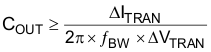
To meet the 60-mV ripple specification, the minimum output capacitance is calculated to be 22.5 µF with Equation 45. This design uses ceramic output capacitors and the effects of ESR are ignored. To meet the transient response of 500 mA with less than 480-mV voltage change and a 7-kHz control loop bandwidth, the minimum output capacitance is calculated to be 23.7 µF using Equation 46. The RMS current is calculated with Equation 22 to be 1.44 A. The output capacitors used in this design are 3 × 22 µF, 25 V, X7R 1210 ceramic capacitors. With voltage derating, the effective total output capacitance is estimated to be 30.4 µF.
Equation 45. 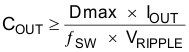
Equation 46.